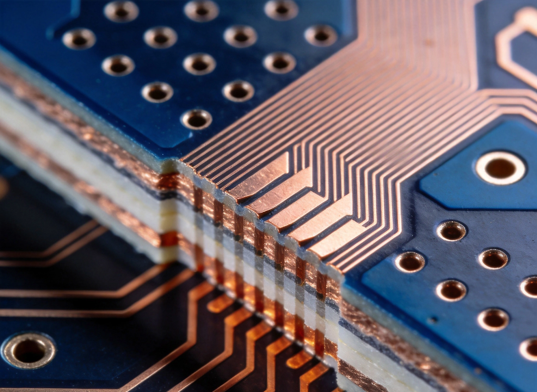
Handling HDI and High-Frequency Materials in 5G PCB Assembly
Home Blog Turnkey PCB Solutions Telecom 5G & High-Speed Computing

Handling HDI and High-Frequency Materials in 5G PCB Assembly

September/17/2026

5G Pcb Design sits at the intersection of two demanding technologies: High-density Interconnect (HDI) for routing the massive I/O counts of modern 5G chipsets, and high-frequency laminate materials for preserving Signal Integrity at Sub-6 GHz and mmWave frequencies. When these two worlds converge on a single board, the assembly challenges multiply—because the processes that benefit HDI (sequential lamination, microvia drilling, fine-line imaging) can conflict with the requirments of high-frequency materials (low Dk tolerance, minimal conductor loss, controlled impedance). Understanding how to handle HDI and high-frequency materials together in 5G Pcb Assembly is essential for building boards that actually work at 28 GHz, 39 GHz, and beyond.

Why 5G Boards Demand Both HDI and High-Frequency Materials

The 5G system architecture creates simultaneous demands for routing density and RF performance that cannot be satisfied by either technology alone.

The HDI Imperative

Modern 5G baseband processors and RF transceiver ICs use fine-pitch BGA packages—0.4 mm pitch with 1,000+ connections is common. Escaping these packages on a conventional PCB would require 14–20 layers with through-hole vias, resulting in an impractically large and thick board. HDI with microvias (0.1–0.15 mm diameter) and via-in-pad enables BGA escape routing in 8–12 layers, reducing both board area and thickness. For 5G user equipment (smartphones, CPE devices) where space is at a premium, HDI is non-negotiable.

The High-Frequency Imperative

5G signals—particularly in the FR2 (mmWave) bands at 24–40 GHz—are extraordinarily sensitive to PCB material properties. Standard FR4 has a dielectric constant (Dk) of approximately 4.5 and a dissipation factor (Df) of 0.02 at 1 GHz. At 28 GHz, the Df effectively increases, causing insertion loss that can exceed 2 dB per inch of trace—rendering the signal unusable over even short interconnect distances. High-frequency laminates (Rogers RO4003C, RT/Duroid 5880, Panasonic Megtron6) offer Dk values of 3.0–3.5 with Df below 0.003, reducing insertion loss to manageable levels.

The challenge: these two imperatives must coexist on the same board. The baseband processing section needs HDI routing density. The RF front-end and antenna interface need low-loss high-frequency materials. Making them work together is the core engineering problem of 5G Pcb Assembly.

Material Selection for Mixed HDI/High-Frequency 5G Boards

The first critical decision is material selection—specifically, how to partition the board between HDI construction layers and high-frequency layers.

Common 5G PCB Material Systems

  • All-FR4 with localized RF sections: The simplest approach uses FR4 throughout but specifies low-loss FR4 variants (Isola 370HR, Megtron6) for the RF-critical layers. This avoids the complexity of mixed-material lamination but accepts higher insertion loss for RF traces. Suitable for Sub-6 GHz designs where loss budgets are more forgiving.
  • FR4 core with Rogers build-up: A conventional FR4 core provides the mechanical and routing foundation, while Rogers or equivalent material is used as build-up layers on one or both sides for the RF circuitry. This is the most common approach for 5G base station boards.
  • Mixed-material stack-up: Different layers use different materials within the same lamination—FR4 for routing-dense digital layers, Rogers or Megtron6 for RF layers. This is the highest-performance approach but the most challenging to manufacture.

Material Compatibility Considerations

When different materials are laminated together, their coefficient of thermal expansion (CTE), glass transition temperature (Tg), and decomposition temperature (Td) must be compatible:

  • CTE mismatch: FR4 has a CTE of approximately 14–17 ppm/°C in the X-Y plane, while Rogers RO4003C is approximately 11 ppm/°C. This mismatch creates stress at the material interface during thermal cycling, potentially causing delamination. The Z-axis CTE mismatch is even more critical—FR4's Z-axis CTE (50–70 ppm/°C above Tg) is much higher than PTFE-based materials, stressing plated through-holes at the material boundary.
  • Tg compatibility: FR4 has a Tg of 130–180°C depending on grade, while PTFE-based materials like Rogers have no true Tg—they remain dimensionally stable to much higher temperatures. During lamination, the FR4 layers flow and cure at temperatures that may be above the PTFE material's recommended processing range, potentially altering its electrical properties.
  • Pressure sensitivity: PTFE-based materials are compressible under lamination pressure. Excessive pressure during sequential lamination can reduce the dielectric thickness, altering the impedance of controlled RF traces. Lamination recipes for mixed-material boards must be carefully developed to apply sufficient pressure for FR4 resin flow without compressing the RF layers.

Lamination Challenges for Mixed-Material HDI

Lamination is where the HDI and high-frequency requirements most directly conflict. HDI construction typically uses sequential (build-up) lamination—each microvia layer pair is laminated, drilled, and plated separately. High-frequency materials demand consistent dielectric thickness and minimal resin flow variation to maintain Impedance Control.

Sequential Lamination with Mixed Materials

In a typical 5G HDI board, the construction sequence might be:

  1. Laminate the FR4 core (layers 3–6, for example) with conventional through-hole vias.
  2. Drill and plate through-holes in the core.
  3. Laminate the first build-up layer pair (Rogers on one side, FR4 build-up on the other).
  4. Laser drill microvias in the build-up layers.
  5. Plate and fill microvias.
  6. Repeat for additional build-up layers.

Each lamination cycle subjects the board to approximately 180°C and 200–400 PSI for 60–90 minutes. For PTFE-based materials, this repeated thermal cycling can cause gradual changes in dielectric properties—Dk can shift by 1–2% after multiple lamination cycles, which directly affects impedance for RF traces. The process engineer must account for this drift when specifying the initial dielectric thickness.

Resin Flow Control

During lamination, FR4 prepreg resin flows to fill voids and bond layers. In mixed-material constructions, this resin flow must be contained to prevent FR4 resin from contaminating the RF dielectric layers. Even small amounts of FR4 resin (which has much higher Dk and Df than Rogers) infiltrating the RF dielectric can create localized impedance discontinuities that degrade Signal Integrity at mmWave frequencies.

Controlling resin flow requires:

  • Using low-flow or no-flow prepregs adjacent to RF layers.
  • Specifying adequate copper coverage on the FR4 layers to limit resin flow paths (hatched fills at 50–60% coverage can help).
  • Designing the stack-up so that FR4-to-Rogers interfaces occur at internal ground planes that act as resin flow barriers.

Microvia Reliability in High-Frequency Constructions

Microvias are the hallmark of HDI technology, and their reliability has been the subject of extensive industry investigation. In 5G boards that combine HDI with high-frequency materials, microvia reliability faces additional stressors beyond those in conventional HDI constructions.

CTE-Driven Stress at Material Boundaries

When a microvia connects layers of different materials—for example, a Rogers build-up layer to an FR4 core—the Z-axis CTE mismatch creates stress at the via barrel during thermal cycling. PTFE-based materials have very low Z-axis CTE (typically 20–30 ppm/°C) compared to FR4 (50–70 ppm/°C above Tg). As the board heats and cools, the FR4 expands more than the PTFE, putting tensile stress on the microvia copper plating at the material interface.

This stress mechanism is distinct from the well-known microvia cracking at the capture pad (target pad) interface that has historically plagued HDI reliability. In mixed-material boards, cracking can occur at the material boundary even when the via-to-pad interface is sound. The risk is proportional to the number of thermal cycles the board experiences—making it particularly concerning for 5G infrastructure equipment that operates outdoors with large daily temperature swings.

Mitigation Strategies

  • Copper-filled microvias: Filling microvias with electroplated copper (rather than leaving them hollow or filled with conductive paste) provides a continuous copper structure that is much more resistant to CTE-driven cracking. Copper fill is now considered best practice for any microvia in a mixed-material 5G board.
  • Staggered rather than stacked microvias: Stacked microvias (where one via sits directly on top of another) create a high-stress concentration point. Staggered microvias (offset vertically) distribute the stress across a larger copper area. For mixed-material constructions where CTE mismatch is present, staggered microvias are preferred unless routing density absolutely requires stacking.
  • Reliability qualification testing: IST (Interconnect Stress Test) per IPC-TM-650 2.6.26 and thermal cycling per IPC-9701 should be performed on representative test coupons that include microvias at material interfaces. For 5G infrastructure boards, a minimum of 1,000 thermal cycles from -40°C to +125°C is recommended before qualifying a new HDI/high-frequency stack-up.

Impedance Control at 5G Frequencies

Impedance Control becomes progressively more difficult as frequency increases, and 5G frequencies push the limits of what PCB Fabrication can reliably achieve.

Dk Tolerance and Its Impact on Impedance

The impedance of a microstrip or stripline trace depends on the dielectric constant (Dk) of the surrounding material, the trace width, and the trace-to-reference-plane distance. For a 50Ω microstrip on Rogers RO4003C (Dk = 3.38), a ±0.05 variation in Dk (the material manufacturer's typical tolerance) causes approximately ±0.8Ω impedance variation—manageable for Sub-6 GHz but marginal for mmWave where impedance tolerances of ±5% or tighter are often required.

However, the effective Dk of the dielectric stack-up is not simply the material's nominal Dk. It is influenced by sevral factors:

  • Glass fiber weave effect: The woven glass fabric in FR4 and some RF laminates creates periodic Dk variations as traces pass over glass bundles (higher Dk) versus resin-rich areas (lower Dk). At mmWave frequencies, this micro-scale Dk variation causes impedance modulation along the trace. Low-Dk glass (NE-glass, SI-glass) and spread-glass weaves reduce but do not eliminate this effect.
  • Copper surface roughness: The roughness of the copper foil surface that contacts the dielectric affects the effective Dk and contributes to conductor loss. Standard electrodeposited (ED) copper has surface roughness of 5–10 μm RMS, which is unacceptable for mmWave traces. Low-profile copper (LP copper, 1–3 μm RMS) or reverse-treated copper (RTF, 1–2 μm RMS at the dielectric interface) is required for 5G RF layers.
  • Resin content variation: The ratio of resin to glass in the laminate affects Dk. Process variations in laminate manufacturing cause resin content to vary by ±2–3%, translating to Dk variations that impact impedance.

Design Strategies for Tight Impedance Control

  • Use homogeneous RF dielectrics: PTFE-based laminates (Rogers RT/Duroid, Taconic RF-35) are not reinforced with glass fabric—they are homogeneous materials with no weave effect. This eliminates the largest source of Dk variation in the RF section of the board.
  • Specify low-profile copper on RF layers: Request LP or VLP copper foil for all layers that carry controlled-impedance RF traces. The slightly higher cost is justified by significantly lower conductor loss and more predictable impedance at 5G frequencies.
  • Design wider traces on thinner dielectrics: For a given impedance target, using a thinner dielectric allows wider traces that are less sensitive to etching tolerance. A 50Ω microstrip on a 3.4 mil dielectric requires approximately 5.5 mil trace width—a ±0.5 mil etching tolerance causes ±4.5Ω impedance variation. The same 50Ω on an 8 mil dielectric requires an 11 mil trace, where ±0.5 mil tolerance causes only ±2.2Ω variation.
  • Include impedance test coupons: Every production panel should include test coupons that replicate the RF stack-up with representative trace geometries. Time-domain reflectometry (TDR) measurement of these coupons validates that the fabricated impedance matches the design target within tolerance.

Conductor Loss and Surface Finish Selection

At 5G frequencies, conductor loss becomes a significant fraction of total insertion loss—and the PCB surface finish directly affects conductor loss for RF traces on outer layers.

Surface Finish Impact on RF Performance

The surface finish is the thin metallic coating applied to exposed copper pads and traces to prevent oxidation and ensure solderability. Different finishes have different impacts on RF performance:

  • ENIG (Electroless Nickel / Immersion Gold): The nickel layer (3–5 μm) has approximately 3× the resistivity of copper at DC, and its skin-depth performance at GHz frequencies is significantly worse. For a microstrip trace at 28 GHz, ENIG can add 0.3–0.5 dB/inch of insertion loss compared to bare copper. This is substantial for mmWave traces that may be several inches long. ENIG also introduces a "nickel dip" in insertion loss versus frequency that can create unexpected performance variation across a wideband 5G signal.
  • Immersion Silver: A thin silver layer (0.1–0.3 μm) over copper provides solderability with minimal impact on RF performance—silver is actually a better conductor than copper at RF frequencies. The disadvantage is limited shelf life (6–12 months) and sensitivity to sulfur contamination in storage.
  • Immersion Tin: Similar thickness to immersion silver but tin has higher resistivity than copper. The RF penalty is intermediate between ENIG and immersion silver.
  • OSP (Organic Solderability Preservative): A thin organic coating that protects the copper surface. OSP provides the best RF performance because the RF current flows on essentially bare copper. However, OSP is not suitable for multiple reflow cycles or long storage, limiting its use in complex double-sided assemblies.

The practical recommendation for 5G boards: use immersion silver on outer layers for the best balance of RF performance, solderabilty, and shelf life. Avoid ENIG on outer layers that carry mmWave RF traces. If ENIG is required for specific components (wire-bondable areas, press-fit connectors), use selective plating to limit ENIG to those areas only.

Solder Paste and Reflow Considerations for 5G HDI

Assembly of 5G HDI boards presents specific soldering challenges related to the combination of fine-pitch components, mixed-material construction, and thermal sensitivity of RF dielectrics.

Fine-Pitch Solder Paste Printing

5G chipsets use 0.4 mm pitch BGAs with pad sizes of 0.2–0.25 mm. Successfully printing Solder Paste on these pads requires:

  • Type 4 or Type 5 Solder Paste: Type 4 (20–38 μm particle size) is the minimum for 0.4 mm pitch. Type 5 (10–25 μm) provides better print definition for 0.35 mm pitch and below. The finer particle size increases cost and reduces solder paste working life (pot life and stencil life).
  • Fine-pitch Stencil Design: Stencil apertures for 0.4 mm pitch BGA pads are typically 0.18–0.20 mm on a 0.10–0.12 mm thick stencil. Area ratio (aperture area divided by aperture wall area) must exceed 0.66 for reliable paste release. Nano-coated stencils (electropolished with a hydrophobic coating) significantly improve paste release at these dimensions.
  • SPI (Solder Paste Inspection): 100% Spi Inspection after paste printing is essential for 5G HDI boards. The cost of a solder defect on a $50 RF IC is too high to rely on statistical process control alone.

Reflow Profile Constraints

The reflow profile must simultaneously satisfy the requirements of the solder paste (peak temperature, time above liquidus) and the limitations of the PCB materials:

  • PTFE material temperature limits: PTFE-based laminates can begin to outgas or experience dimensional changes at temperatures above 260°C. A reflow profile with a peak temperature of 245–250°C (appropriate for SAC305 solder paste) is generally safe, but profiles approaching 260°C risk PTFE degradation.
  • Maximum reflow passes: Each reflow cycle subjects the board to thermal stress that affects both microvia reliability and RF material properties. Mixed-material HDI boards should be designed to minimize the total number of reflow passes—preferably single-pass reflow for SMT components, with through-hole components soldered by Selective Soldering rather than a second reflow.
  • Vacuum reflow for BGA voiding: 5G RF BGAs are particularly sensitive to solder voids, which interrupt both the electrical and thermal path beneath the die. Vacuum reflow during the liquidus phase can reduce void percentages to below 5%, but the vacuum cycle adds time at elevated temperature—ensure the total TAL (time above liquidus) remains within material limits.

Inspection Challenges Specific to 5G HDI Assembly

Quality inspection of 5G HDI boards requires tools and techniques beyond standard PCBA inspection.

X-Ray Inspection for RF BGA Joints

The RF transceiver ICs in 5G boards use large-area BGA packages where the thermal and electrical performance of every solder joint is critical. X-ray inspection (2D or 3D) must evaluate:

  • Void percentage within each solder joint (target below 5% for thermal pads beneath the die).
  • Solder joint geometry and coplanarity across the BGA.
  • Microvia connectivity beneath BGA pads (via-in-pad construction means the X-ray can verify that the microvia is properly filled and connected).

RF-Specific Functional Testing

Conventional ICT and FCT verify digital logic and power functionality but do not measure RF performance. For 5G boards, RF-specific testing is essential:

  • Insertion loss and return loss: Vector Network Analyzer (VNA) measurement of RF trace paths to verify that the fabricated insertion loss matches the design simulation. Discrepancies indicate material Dk variation, etching tolerance issues, or surface finish problems.
  • Isolation between MIMO paths: Massive MIMO 5G architectures require high isolation (>30 dB) between adjacent transceiver paths. Measuring Crosstalk on the assembled board validates that the PCB layout and component placement achieve the required isolation.
  • Antenna impedance match: For mmWave modules with on-board antenna structures, the impedance match at the antenna feed point must be verified after assembly—solder joints, component placement, and even Conformal Coating can affect the antenna match.

Design for Manufacturability (DFM) Best Practices

Proactively addressing manufacturability during design reduces the risk and cost of 5G HDI/high-frequency assembly:

  • Separate digital and RF routing layers: Use dedicated layers for high-speed digital signals (controlled impedance, but tolerant of standard FR4) and separate layers for RF signals (requiring low-Dk, low-Df material). This simplifies the stack-up and reduces the number of material transitions.
  • Avoid RF traces on mixed-material interfaces: Route RF traces entirely within one material system (e.g., fully within the Rogers build-up layers) rather than transitioning between materials. Material transitions create impedance discontinuities that are difficult to predict and impossible to tune after fabrication.
  • Provide adequate clearance around RF components: RF matching networks, filters, and antenna structures are sensitive to nearby copper patterns and component placement. Define keep-out zones in your design rules that prevent routing or copper fill from encroaching on RF-critical areas.
  • Use via fencing for Rf Shielding: Rows of ground vias (via fences or picket fences) along the boundaries of RF trace channels provide shielding between adjacent RF paths. Specify via spacing of λ/20 or less at the highest operating frequency for effective isolation.
  • Document material specifications explicitly: Do not assume the fabricator will select the right material. Specify the exact laminate grade, prepreg type, copper foil profile, and surface finish for each layer in your fabrication drawing. For mixed-material boards, include a stack-up diagram showing which layers use which materials.

Conclusion

Handling HDI and high-frequency materials together in 5G PCB assembly requires careful coordination across design, material selection, fabrication, and assembly processes. The routing density demands of 5G chipsets necessitate HDI construction with microvias and sequential lamination, while the signal integrity requirements of Sub-6 GHz and mmWave RF paths demand low-loss dielectrics, low-profile copper, and impedance control tolerances measured in fractions of an ohm. The challenges of combining these technologies—CTE mismatch at material boundaries, microvia stress at mixed-material interfaces, Dk tolerance accumulation, and conductor loss from surface finishes—are substantial but manageable with deliberate engineering and process control.

Success in 5G HDI/high-frequency assembly comes from treating the PCB as an RF component—not just a mechanical substrate for component mounting. Every material choice, every via construction, every surface finish decision, and every lamination parameter effects the RF performance of the finished board. Designing and specifying with this understanding—and partnering with a manufacturer who has demonstrated capability in both HDI and high-frequency PCB production—is the foundation of reliable 5G hardware.

For 5G hardware teams seeking a manufacturing partner, working with an experienced PCBA provider that maintains dedicated HDI and RF fabrication lines, with validated mixed-material lamination processes and in-house RF test capability, eliminates the learning curve that causes first-project failures and delays.

FAQ

Can I use standard FR4 for all layers of a 5G PCB?

For Sub-6 GHz designs with short RF trace lengths (under 1 inch), low-loss FR4 variants (Megtron6, Isola 370HR) may provide adequate performance. However, any RF trace longer than 1–2 inches or any mmWave application (24 GHz and above) requires dedicated low-loss material on the RF layers. Using standard FR4 at mmWave frequencies results in insertion loss that exceeds the link budget, making the design non-functional regardless of how well the digital routing works.

What is the cost premium for mixed-material 5G HDI boards?

Mixed-material boards with Rogers or equivalent RF layers cost 3–5× more than all-FR4 boards of the same layer count and dimensions, depending on the proportion of RF material and the HDI construction type. The cost is driven by the expensive RF laminate material ($20–40 per square foot vs. $2–4 for FR4), the complexity of mixed-material lamination, and the additional inspection and testing required. However, this cost is a small fraction of the total 5G module bill of materials, where the RF ICs alone may cost $20–50 per unit.

How do I specify a mixed-material stack-up?

Provide a detailed stack-up diagram showing the material type, thickness, copper weight, and copper foil profile for each layer. Specify the prepreg type and resin content for each bonding interface. Include impedance targets and tolerances for all controlled-impedance traces. For mixed-material constructions, also specify the lamination sequence (which layer pairs are laminated together in each press cycle) to ensure the fabricator understands the intended construction order.

Are stacked microvias reliable in mixed-material 5G boards?

Stacked microvias can be reliable in mixed-material constructions if they are copper-filled (not conductive-paste-filled) and if the stack-up is qualified with appropriate reliability testing (IST and thermal cycling). However, the CTE mismatch at material interfaces adds risk. Many 5G hardware developers prefer staggered microvias with overlap (where adjacent-layer vias overlap in the capture pad area without being directly stacked) as a compromise that provides similar routing density with lower stress concentration.

What solder paste type is recommended for 0.4 mm pitch 5G BGAs?

Type 4 solder paste (20–38 μm particle size) is the standard recommendation for 0.4 mm pitch. Type 5 (10–25 μm) provides better print definition for 0.35 mm and finer pitches but has shorter working life and higher cost. For 5G HDI boards, the choice between Type 4 and Type 5 should be validated with paste printing trials on the actual Stencil Design, as print quality depends on the interaction between paste type, stencil aperture geometry, and stencil surface treatment.
Send Message
Name*
E-mail*
Country*
Phone/WhatsApp*
Name*
E-mail*
Country*
Phone/WhatsApp*