
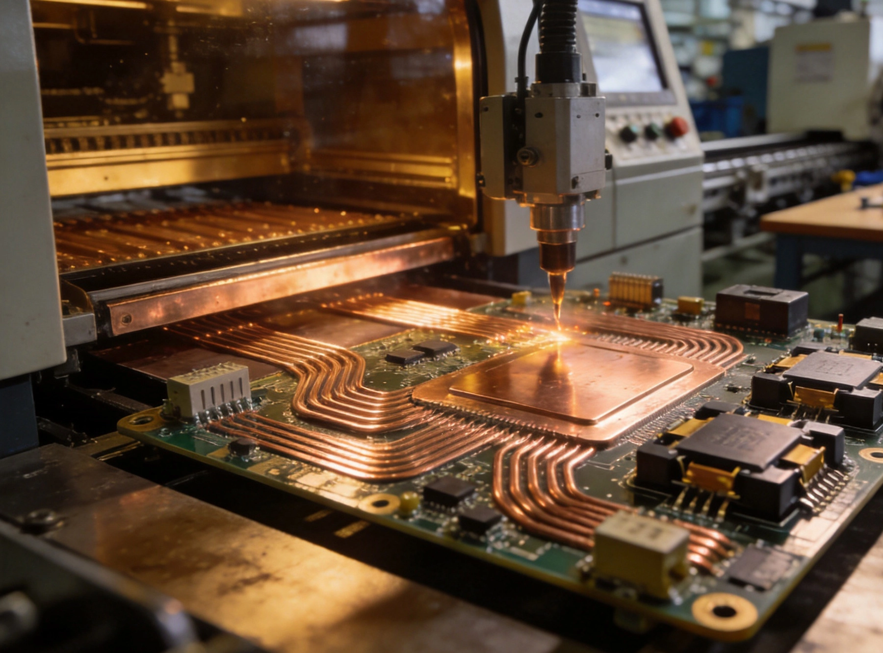
Heavy copper PCBs serve demanding power electronics applications where standard copper weight cannot provide adequate current capacity or thermal performance. These boards, typically featuring 3oz to 20oz copper or even thicker, appear in power supplies, motor controls, Automotive Electronics, and renewable energy systems. While heavy copper provides essential electrical and thermal capabilities, it introduces significant challenges during Pcb Assembly that require specialized processes and careful attention to detail.
Standard PCB copper weight measures one ounce per square foot, producing approximately 1.4 mils (35μm) finished thickness. Heavy copper boards start at three ounces per square foot and may reach twenty ounces or more, creating conductors that can carry dramatically higher current while offering superior thermal spreading. This capability comes with tradeoffs in manufacturing complexity and assembly difficulty.
Applications driving heavy copper adoption include electric vehicle chargers requiring hundreds of amperes, solar inverters managing kilowatt-level power flow, and industrial motor drives where thermal management determines system reliability. These applications cannot function with standard PCB copper weights, making heavy copper a necessity rather than an option.
The transition zone between heavy copper and standard circuitry presents particular challenges. Power distribution networks often incorporate both high-current bus bars and low-power control circuits on the same board. Managing this transition requires careful planning to ensure that assembly processes accommodate both extremes without compromising either.
Via formation in heavy copper boards demands specialized plating processes to achieve reliable barrel plating throughout deep holes. Standard PCB plating may produce acceptable results for aspect ratios up to approximately 8:1, but heavy copper boards often require aspect ratios exceeding this threshold. The resulting plating uniformity challenges can cause voids, cracks, or insufficient copper thickness in via barrels.
Via-in-pad with heavy copper presents additional complications. Standard tenting and plugging processes might not seal heavy copper vias effectively, allowing solder to wick into barrel cavities during assembly. This wicking can deplete solder from joints while creating potentially unreliable connections. Filled and capped via processes address these concerns but add significant cost to board pricing.
Thermal via arrays surrounding high-power components require careful design to balance thermal performance against manufacturing feasibility. Via density affects drilling time and plating capacity, with extremely dense arrays potentially exceeding manufacturer capabilities. Design consultation helps identify achievable thermal via configurations that meet thermal requirements while remaining manufacturable.
Solder Paste Printing on heavy copper boards requires adjusted parameters compared to standard circuitry. The topography created by heavy copper traces produces uneven surfaces that challenge squeegee blade contact and paste deposition. Standard print parameters developed for flat substrates may produce inconsistent volume and coverage on heavy copper boards.
Paste selection influences printing success on non-uniform surfaces. No-clean formulations with appropriate viscosity and slump resistance perform better across uneven topography. Some assemblers prefer solder paste with smaller particle size (Type 4 or Type 5) to improve filling into narrow spaces between heavy copper features.
Print speed and squeegee pressure require optimization for heavy copper substrates. Slower print speeds allow paste to flow more completely into irregular surface features. Increased squeegee pressure ensures blade contact despite topography variations, though excessive pressure can cause paste extrusion beyond pad boundaries.
Component placement on heavy copper boards must account for surface irregularities that shift effective component positions. Optical recognition systems that reference pad edges can compensate for surface topology variations, but placement systems relying solely on absolute coordinates may experience increased placement offset errors.
Heavy components such as large MOSFETs, IGBT modules, and transformers impose mechanical stresses that can shift during reflow if attachment methods do not account for weight. These components require either robust temporary holding mechanisms during Solder Reflow or adhesive pre-attachment before paste printing.
Fine-pitch components placed in areas surrounding heavy copper features face particular challenges. The height differential between heavy copper regions and standard circuitry can cause stencil gap issues during printing or interference with placement heads. Careful component placement planning that considers height constraints improves assembly success rates.
Reflow profile development for heavy copper boards must account for increased thermal mass that slows temperature ramp rates. Standard profiles optimized for thin, uniform boards may produce insufficient time-above-liquidus when applied to heavy copper assemblies. Extended soak periods help ensure that component and heavy copper regions reach equilibrium temperature before reflow.
Heavy copper acts as a heat sink during Solder Reflow, drawing heat away from component termination areas faster than standard circuitry. This thermal shunting effect can prevent proper solder wetting, producing cold joints or incomplete connections. Profile adjustment to increase peak temperature or extend time-above-liquidus addresses this concern.
Component proximity to heavy copper regions affects thermal exposure during reflow. Components positioned directly adjacent to heavy copper planes experience different thermal profiles than those surrounded by standard circuitry. Mapping thermal conditions across the board surface guides profile optimization that accommodates regional variations.
Heavy copper boards require attention to thermal gradients that can cause component damage during assembly. Uneven heating during reflow creates stress concentrations that may crack ceramic components or delaminate substrates. Careful profile development that minimizes temperature gradients across boards reduces these risks.
Preheating considerations become more critical for heavy copper assemblies. Gradual preheat ramps allow temperature equilibration between components and substrates, reducing thermal shock risks. Extended preheat periods also drive off moisture absorbed by components and boards, preventing popcorn defects that can occur during rapid reflow heating.
Cooling rate control after reflow affects solder joint microstructure and reliability. Forced air cooling that rapidly reduces board temperature may introduce thermal gradients causing component stress. Controlled cooling that follows predictable rates produces more consistent joint structures while reducing residual stress in assemblies.
Heavy copper boards often require through-hole components for high-current connections, presenting unique assembly challenges. Wave Soldering processes must achieve adequate solder penetration into heavy copper barrels, which present larger thermal mass than standard PCB barrels. Preheating and wave temperature require adjustment to ensure proper solder flow.
Selective Soldering processes provide alternative approaches for through-hole components on heavy copper boards. These processes apply solder precisely where needed without exposing entire boards to wave temperatures, reducing thermal stress and energy consumption. Programming selective solder tools requires careful setup to accommodate heavy copper thermal characteristics.
Press-fit pins offer advantages for high-current through-hole connections without requiring solder. The mechanical interference fit between press-fit pins and heavy copper barrel walls provides reliable electrical connection while eliminating solder-related assembly concerns. Press-fit technology requires appropriate barrel finished diameter and plating specifications to achieve reliable connections.
Heavy copper board inspection requires adjusted acceptance criteria that account for manufacturing realities. Standard IPC inspection criteria developed for thin copper boards may not apply directly to heavy copper features. Visual inspection standards should reference appropriate specifications for heavy copper assemblies.
X-ray inspection proves essential for verifying solder joint quality in heavy copper assemblies. The high-density copper surrounding solder joints requires appropriate X-ray energy to penetrate and reveal internal joint structure. Lower-energy X-ray systems may produce insufficient penetration for thick copper boards, creating blind spots in inspection coverage.
Electrical testing verifies connectivity and isolation, but test probe contact force must be sufficient to penetrate any oxide that forms on heavy copper surfaces. Standard test equipment with minimal probe force may produce unreliable readings on heavy copper test points. Establishing appropriate test parameters ensures accurate verification of heavy copper assemblies.
Rework operations on heavy copper boards face challenges exceeding those for standard assemblies. The thermal mass of heavy copper regions creates significant heat sinks that prevent localized heating sufficient for component removal. Hot air rework stations may struggle to achieve temperatures adequate for solder reflow when heavy copper draws heat away from the work area.
Component removal may require heating the entire board rather than localized rework zones. This approach risks damage to temperature-sensitive components not intended for removal, complicating rework operations. Pre-heating platens that warm boards to elevated temperatures reduce the thermal differential that complicates rework.
Replacement component installation requires attention to heavy copper thermal characteristics during solder reflow. The heat sinking effect that complicates removal also affects solder wetting during installation. Profile adjustment to increase thermal input ensures reliable joint formation when installing replacement components.
Not all contract manufacturers possess capabilities for heavy copper assembly. Before selecting a partner, verify relevant experience with your specific copper weight and application requirements. Ask for sample boards demonstrating capability and inquire about failure rates for comparable projects.
Equipment capabilities influence achievable results for heavy copper assembly. Assemblers with modern reflow ovens offering precise temperature control can better accommodate heavy copper thermal characteristics. Older equipment with limited profile flexibility may produce inconsistent results.
Quality system certifications provide additional confidence in assembly capability. ISO 9001 certification indicates basic quality management competence, while industry-specific certifications demonstrate expertise relevant to particular applications. Iatf 16949 for automotive or AS9100 for aerospace indicate capabilities beyond standard commercial assembly.
Heavy copper Pcb Assembly presents challenges that differ significantly from standard circuitry. The electrical and thermal capabilities that make heavy copper essential also create manufacturing complexities requiring specialized approaches. Understanding these challenges enables designers to create assemblies that meet both performance requirements and manufacturing realities.
Successful heavy copper assembly results from collaboration between designers, fabricators, and assemblers. Early engagement with manufacturing partners helps identify potential issues before production commitments. Design optimization informed by manufacturing feedback produces more reliable outcomes than attempting to manufacture designs without this input.
The investment required to accommodate heavy copper assembly challenges yields returns through reliable power electronics that perform throughout their intended service life. By addressing assembly considerations during design rather than discovering problems during production, engineers can achieve successful outcomes that meet demanding application requirements.
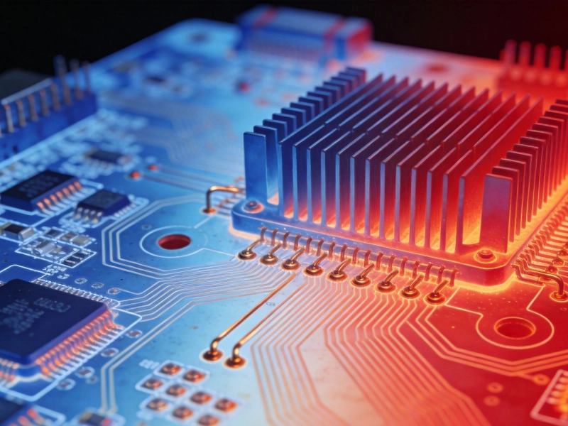
Thermal Management Techniques in Power Electronics PCB AssemblyJuly/16/2026
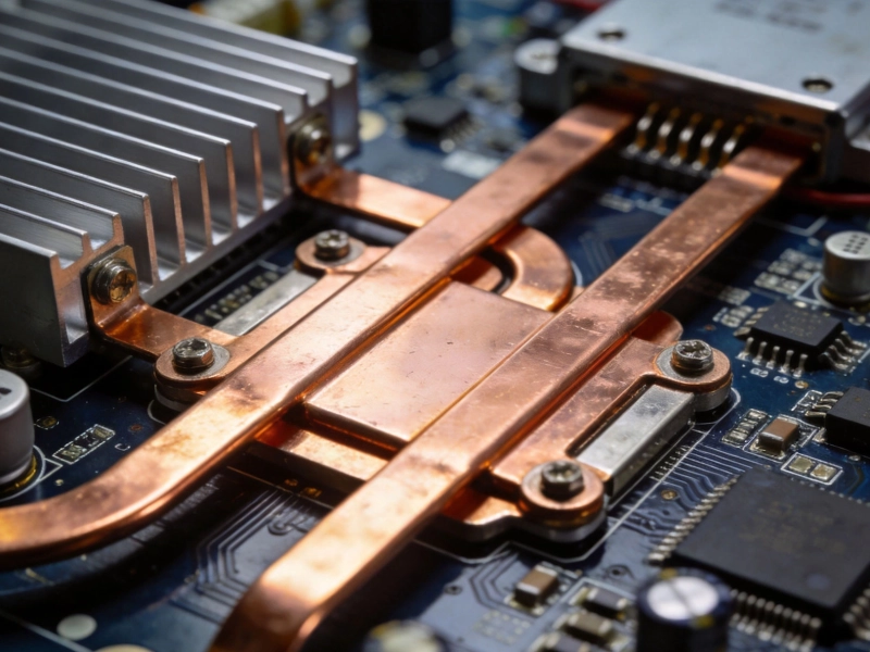
Best Turnkey PCB Assembly for Energy & Power Electronics: Handling High VoltageJune/17/2026
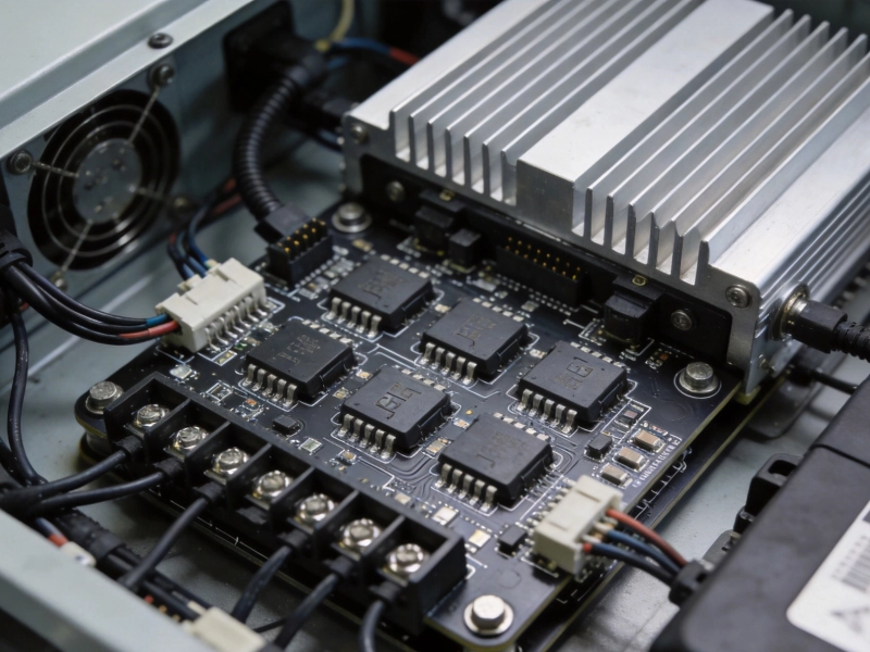
Best Turnkey PCB Assembly for EV Charging Stations and InvertersSeptember/15/2026
Custom Turnkey PCB Solutions for Harsh Environment ApplicationsSeptember/11/2026
Ruggedized PCB Assembly for Harsh Industrial EnvironmentsJuly/20/2026
Supply Chain Resilience in High Volume Turnkey PCBA ProjectsJuly/10/2026
Turnkey PCB Assembly for Flight Control Systems and Navigation<June/22/2026
Cost Reduction Techniques for High Volume Turnkey PCBA OrdersAugust/03/2026