

As computing systems push toward higher data rates and faster edge speeds, the humble printed circuit board transforms from a simple interconnection substrate into a complex electromagnetic environment where signals behave in ways that defy intuition. Signal integrity—the discipline of ensuring electrical signals arrive at their destinations with sufficient quality for reliable operation—has become one of the most critical challenges in high-speed computing Pcb Assembly.
At low frequencies, traces behave as simple wires. At gigabit-per-second data rates, these same traces become transmission lines whose behavior depends on geometry, material properties, and termination. Getting signal integrity right separates functioning systems from frustrating debug sessions and costly respins. Understanding the fundamental challenges prepares engineers to design and assemble PCBs that perform reliably at speed.
A PCB trace becomes "high-speed" when its electrical length approaches the rise time of the signals it carries. When signal edge transitions complete in distances shorter than the trace length, traditional lumped-circuit analysis breaks down. Engineers commonly consider a trace high-speed when propagation delay exceeds one-sixth of the signal rise time, though this threshold varies based on accuracy requirements.
The consequences of high-speed behavior manifest in several ways. Reflections occur when trace impedance mismatches cause portions of the signal to bounce back and forth. Crosstalk couples energy between adjacent traces. EMI radiation increases as signal spectral content extends to frequencies where trace dimensions become significant compared to wavelength. Each phenomenon requires different mitigation approaches during design and assembly.
Computing applications demand ever-increasing data rates that push more designs into high-speed territory. Server interconnects operating at 25 Gbps and 56 Gbps, memory interfaces approaching 6.4 Gbps, and peripheral connections at 5 Gbps and 10 Gbps all require careful signal integrity engineering. What qualified as "high-speed" a decade ago now represents commodity performance.
This escalation forces signal integrity considerations earlier in the design cycle than ever before. Architects selecting interfaces, schematic designers choosing termination schemes, and layout engineers controlling impedance all must understand signal integrity implications. Assembly processes that were adequate for low-speed designs may introduce variations that degrade high-speed performance.
Transmission lines on PCBs have characteristic impedance determined by the geometry of the trace and its relationship to reference planes. For microstrip traces on outer layers, impedance depends on trace width, copper thickness, dielectric thickness, and the dielectric constant of the substrate material. Stripline traces between planes have different relationships involving trace width, dielectric thickness to each plane, and the fill of the space between planes.
Controlling impedance within tight tolerances ensures that signals experience consistent behavior across the board. Typical requirements specify impedance within 10% of target, with critical interfaces demanding 5% or tighter control. Achieving this control requires careful material selection, precise trace geometry, and manufacturing processes that maintain consistency across production panels.
Pcb Stack-up design establishes the foundation for controlled impedance. The sequence and thickness of dielectric materials determines the impedance values achievable with specific trace geometries. High-speed designs typically employ uniform dielectric constants throughout the stack-up, avoiding materials with significantly different properties that would complicate impedance calculations.
Planning the stack-up early in design enables optimization for both impedance control and other requirements like cost and manufacturability. The impedance requirements for various signals—single-ended, differential, power delivery—must be mapped to appropriate layer assignments and trace geometries before layout begins. Late changes to stack-up geometry invalidate earlier impedance calculations and require design re-verification.
Crosstalk occurs when energy couples from one trace to adjacent traces through capacitive and inductive mechanisms. Capacitive coupling transfers energy through the electric field between nearby conductors, while inductive coupling transfers energy through magnetic fields around current-carrying traces. Both mechanisms contribute to total crosstalk, with their relative importance depending on trace geometry and signal characteristics.
Forward crosstalk propagates in the same direction as the aggressor signal and adds to victim trace voltage during the edge transition. Backward crosstalk travels toward the signal source and can reach significant amplitudes depending on coupling length. At high speeds, these effects accumulate over trace lengths that allow multiple transitions to interact, potentially creating false switching on victim traces.
Physical separation between traces directly reduces capacitive coupling. Industry guidelines typically recommend spacing of at least three times the trace width between non-related signals. Differential pairs require tight spacing between the positive and negative conductors but benefit from wider spacing to other signals. Guard traces—grounded traces between signal traces—provide additional isolation for critical nets.
Layer assignment affects crosstalk for stripline traces. Traces on adjacent layers routed perpendicular to each other experience less coupling than parallel traces. Routing sensitive signals on inner layers provides shielding from external fields. These routing strategies require coordination between schematic and layout phases to ensure signal integrity requirements are addressed before physical design begins.
Impedance discontinuities occur wherever trace geometry changes abruptly. Vias transitioning between layers create impedance mismatches due to their geometry and the clearance holes in reference planes. Pads for component terminations add capacitance that locally lowers impedance. Connectors and their mounting patterns often have impedance significantly different from the traces they connect.
The severity of reflection effects depends on the magnitude of impedance mismatch and the time duration of the discontinuity relative to signal rise time. Short discontinuities may cause negligible degradation for slow edges but create significant ringing for fast transitions. As rise times decrease, even small discontinuities produce observable effects on the signal waveform.
Termination at the receiving end of a transmission line absorbs reflected energy before it can return to the source. The most common termination schemes include parallel termination to the reference voltage, series termination at the driver, and Thevenin termination using a voltage divider. Each approach offers different benefits and drawbacks regarding power consumption, component count, and DC biasing.
Parallel termination places a resistor equal to the characteristic impedance between the signal line and its reference plane. This approach effectively absorbs reflections but draws constant current, increasing power consumption. Series termination places resistance in series with the driver output, absorbing reflections at the source. Series termination works best for point-to-point connections where only one receiver exists on the net.
High-speed circuits require stable supply voltages despite rapidly changing current demands. The power delivery network (PDN) must maintain impedance below target values across the frequency range where circuit current noise exists. This requirement spans from DC for load current, through mid-frequency switching noise, to RF frequencies associated with fast transients.
Decoupling capacitors provide local charge storage that supplies current during transients while the main power network responds. The effectiveness of decoupling depends on capacitor selection, placement, and connection to the PDN. Different capacitor values address different frequency ranges, with smaller capacitors handling higher frequencies due to their lower series inductance.
When multiple outputs switch simultaneously, their combined current draw creates voltage fluctuations in the PDN. These simultaneous switching noise (SSN) or ground bounce effects cause the local ground reference to move relative to the system ground. Receivers may interpret these ground shifts as signal level changes, potentially causing data errors.
Managing SSN requires attention to both PDN design and signal routing. Solid reference planes provide low-inductance current return paths that reduce ground bounce magnitude. Symmetric routing for differential signals ensures that both conductors experience the same reference potential shifts. Package and die-level design also affect SSN performance, particularly for components where internal power distribution is not visible to the board designer.
Pcb Manufacturing introduces variations in trace width, spacing, and dielectric thickness that affect impedance and coupling. Etching processes over-etch traces relative to design intent, with the effect being more pronounced for narrow traces. Dielectric thickness varies across panels and between production lots. These variations accumulate to create impedance tolerances that must be accommodated in design margins.
Design rules for controlled impedance typically increase trace widths and spacings beyond minimum manufacturable values to provide margin for variation. Working with fabrication partners to understand their actual process capabilities enables optimal design rules that balance manufacturing yield against electrical requirements. Some fabricators provide impedance testing of sample boards from each production lot to verify performance.
Solder mask overcoat changes the effective dielectric environment for outer layer microstrip traces. The mask thickness and dielectric constant modify the trace's capacitance to reference planes, shifting impedance slightly from the pre-mask value. For extremely tight impedance tolerances, mask application may require accounting in the design calculations.
Surface finishes like HASL, ENIG, and OSP change trace thickness and geometry, again affecting impedance. Gold over nickel (ENIG) adds approximately 50 microinches of metal to the trace surface, while HASL can add variable thickness depending on application. These effects are typically small but may matter for the tightest impedance specifications.
Vias introduce impedance discontinuities that require careful management in high-speed designs. The via barrel acts as a small inductor in series with the signal path. The via pad capacitance to adjacent reference planes adds shunt capacitance. The antipad clearance around the barrel creates additional capacitance. Together, these elements form an equivalent circuit that must be considered in high-speed analysis.
Via stub lengths create resonant structures that can severely degrade signals at frequencies where stub length approaches a quarter wavelength. Back-drilled stubs remove unused barrel portions to eliminate stub resonance. For critical signals, designers may specify controlled depth drilling that leaves minimal stub length without the expense of back-drilling.
Reducing via pad diameter minimizes via capacitance. Increasing antipad clearance around the barrel reduces shunt capacitance further. Using blind or buried vias eliminates through-board stubs entirely but increases manufacturing cost. Microvias with smaller diameters reduce capacitance compared to through-hole vias, though with more limited depth capability.
Ground via placement near signal vias provides return current paths that reduce loop inductance. For differential pairs, ground vias flanking each signal via create a more consistent reference environment for both conductors. This care becomes increasingly important as data rates increase, where even small inductances produce measurable effects.
TDR testing injects a fast edge into a trace and measures reflections that reveal impedance discontinuities. The resulting waveform shows impedance profile along the trace length, identifying problem locations with spatial resolution. TDR provides immediate feedback on manufacturing variations and design flaws before they cause field failures.
Performing TDR on production samples validates that the manufacturing process produces impedance within specified tolerances. This testing complements design simulation by revealing actual performance rather than predicted performance. Many fabrication shops offer TDR verification as a value-added service for controlled impedance boards.
Eye diagrams superimpose multiple bit periods of waveform data to reveal aggregate signal quality. The resulting "eye" opening indicates margin available for timing and voltage variations. A widely open eye suggests reliable communication is achievable, while a closed or distorted eye indicates potential reliability problems.
High-speed interfaces specify minimum eye opening requirements that designs must meet. BERT (bit error rate test) equipment generates the patterns and measures bit error rates at specified points in the system. This testing validates system-level performance including transmitter, receiver, and channel effects together.
Signal integrity in high-speed computing Pcb Assembly demands attention from earliest design stages through manufacturing verification. The fundamental challenges—impedance control, crosstalk, reflections, and power delivery—interact in complex ways that require systematic understanding and mitigation. Successful high-speed designs address these challenges through careful stack-up planning, thoughtful routing, appropriate termination, and manufacturing processes that deliver consistent impedance.
Assembly effects on signal integrity, while sometimes overlooked, deserve attention in high-speed designs. Variations in trace geometry, solder mask, and surface finish affect the electrical environment that signals experience. Working with fabrication partners who understand high-speed requirements ensures that manufactured boards deliver the performance that design predicts.
As data rates continue climbing, signal integrity challenges will grow in importance. The techniques and principles discussed here provide a foundation for addressing current high-speed requirements while building expertise for future challenges. Investing in signal integrity knowledge and infrastructure pays dividends across the product development lifecycle.

Best Turnkey PCB Assembly for Data Centers and Server MotherboardsAugust/10/2026
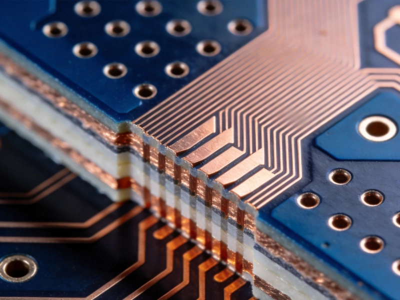
Handling HDI and High-Frequency Materials in 5G PCB AssemblySeptember/17/2026
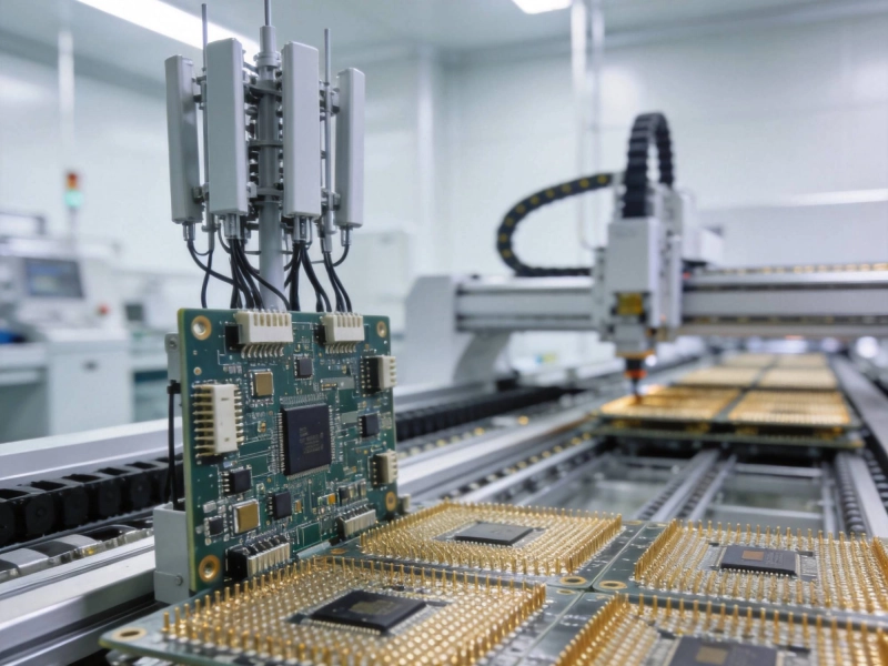
Best Turnkey PCB Assembly for Telecom 5G Infrastructure and Base StationsJune/26/2026

Supply Chain Resilience in High Volume Turnkey PCBA ProjectsJuly/10/2026
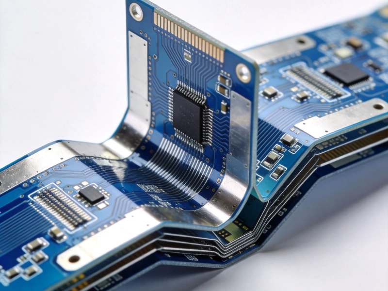
Turnkey PCB Manufacturing for Rigid-Flex and HDI BoardsJuly/08/2026
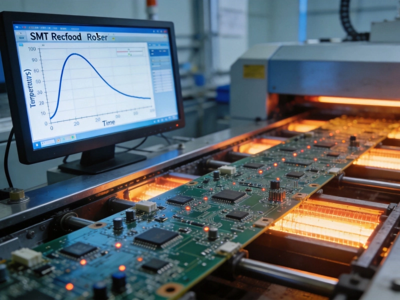
Optimizing Reflow Profiles for Flawless Turnkey SMT AssemblySeptember/30/2026
Best Turnkey PCB Assembly for Complex Multilayer Boards: What to Look ForSeptember/23/2026

Best Turnkey PCB Assembly for Automotive & EV Systems: Meeting IATF 16949June/18/2026