Open Nav

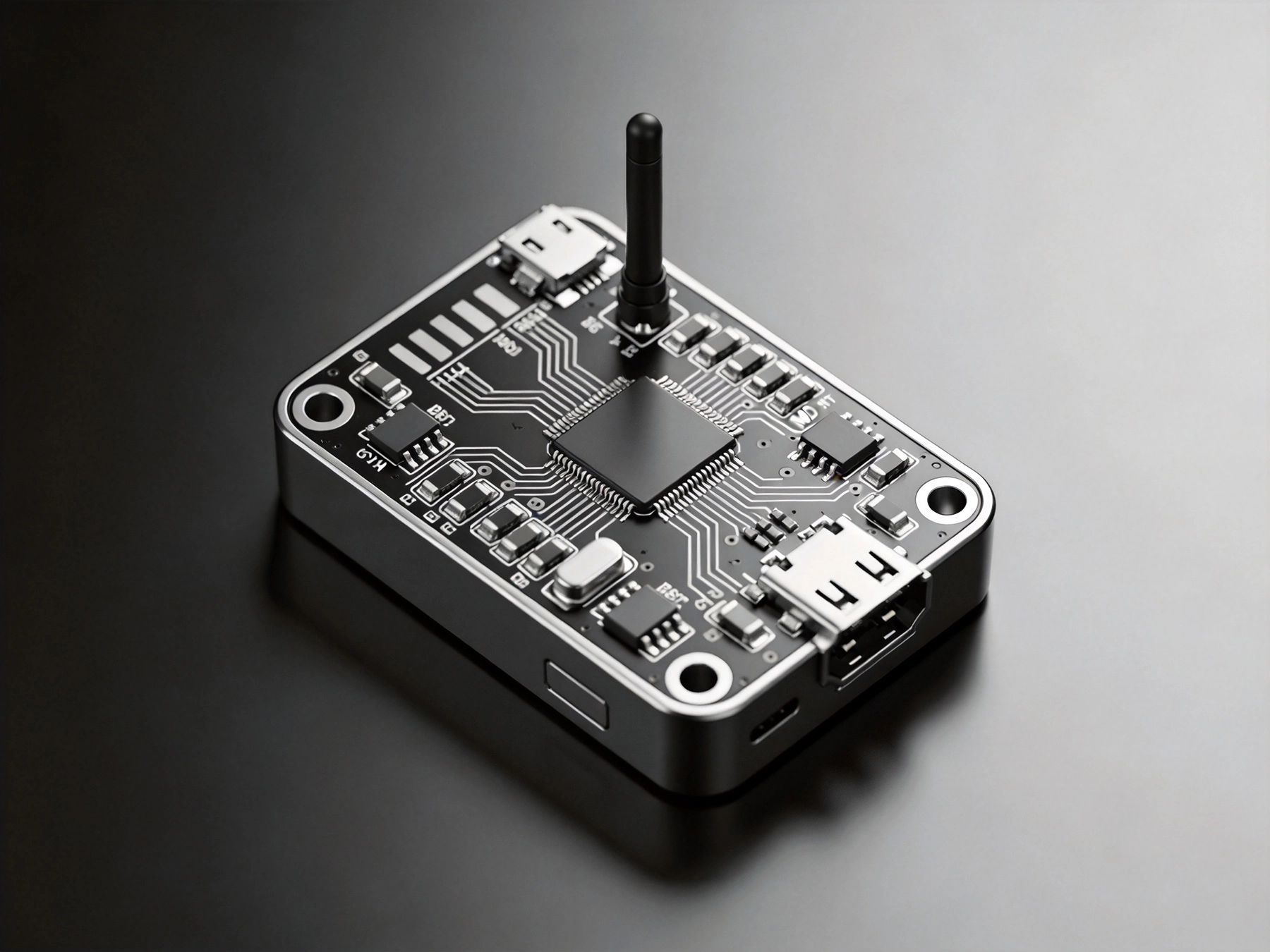
Wireless connectivity is what separates an IoT device from a static electronic product. Whether your board uses Wi-Fi, Bluetooth, Zigbee, LoRa, or cellular, the antenna and RF section of the circuit must work correctly for the device to fulfill its purpose. Getting wireless performance right in a Turnkey Assembly context requires attention to design, fabrication, and assembly details that are easy to overlook when you are focused on bringing a product to market quickly.
Most PCB performance metrics—trace continuity, solder joint integrity, component placement accuracy—are pass/fail. The board either works or it does not. Wireless performance is not like that. It exists on a spectrum. A board might transmit and receive but with reduced range, higher current consumption, or degraded data rates that limit real-world usability. These degradations often do not appear in standard assembly testing, which means they reach customers as field complaints.
In a turnkey context, where one provider handles Design Review, fabrication, assembly, and test, the risk is that the wireless performance requirements are not communicated clearly to the fabricator, or the test coverage does not include RF verification. Understanding what affects wireless performance helps you specify requirements accurately and work with your turnkey partner to ensure adequate testing.
The antenna is the most critical element in any wireless system. For Iot Devices, designers typically choose between three approaches: a trace antenna etched directly on the PCB, a chip antenna mounted on the board, or an external antenna connected via a coaxial connector. Each has trade-offs in cost, performance, and regulatory compliance.
Trace antennas are the lowest cost because they require no separate component, but they demand careful layout. The antenna must have a clear ground clearance area—no components, routing, or copper on adjacent layers—extending at least a quarter wavelength from the radiating element. For 2.4 GHz applications like Bluetooth and Wi-Fi, this clearance zone is roughly 15–20 mm from the antenna edges.
Chip antennas offer better performance in a smaller footprint and provide more predictable RF characteristics than trace antennas, which can vary with PCB material properties and manufacturing tolerances. However, they require matched feed networks and keep-out zones similar to trace antennas, and the component itself adds BOM cost.
External antennas—whether whip, dipole, or PCB-mounted ceramic—typically deliver the best performance and the most flexibility in device industrial design. The trade-off is connector cost, cable assembly complexity, and the need for RF testing that accounts for antenna type and orientation.
The dielectric properties of the PCB substrate directly affect antenna performance and Signal Integrity at RF frequencies. Standard FR-4 has a dielectric constant that varies with frequency and temperature, which can shift antenna impedance and cause detuning. For frequencies above 1 GHz, the material's dissipation factor (Df) also matters because higher Df means more signal loss.
For Wi-Fi and Bluetooth designs, standard FR-4 is generally acceptable if the antenna is a simple design and the board layout is clean. For LoRa, sub-GHz, or cellular applications where narrowband performance matters, consider a high-frequency laminate like Rogers RO4003C or Isola I-Tera. These materials offer stable dielectric constant across frequency and temperature, which translates to more predictable antenna matching.
The stack-up affects RF performance in other ways. Ground plane thickness and placement influence trace impedance and antenna return loss. For controlled impedance RF traces connecting the radio chip to the antenna, maintain consistent spacing to the reference ground plane and use the fabricator's impedance calculator to specify trace width and gap.
High-speed digital signals from the wireless chip can interfere with the antenna if they are routed too close. The crystal oscillator, power supply bypass capacitors, and data lines from the wireless module should be kept away from the antenna region. The datasheet for your wireless module usually specifies keep-out zones—follow them.
For modules with integrated radios, the module manufacturer has already handled most of the RF design. Your responsibility is to provide adequate decoupling, follow the recommended landing pattern, and avoid routing traces under the module that could couple noise into the radio section. The module evaluation board layout is your reference for component placement and routing geometry.
Power supply noise is a common source of reduced wireless performance. Switching regulators can generate noise at frequencies that fall within the operating band of your wireless protocol. If you are using a switching regulator, add sufficient input and output filtering, and consider whether a low-noise LDO regulator for the radio section is worth the thermal cost.
In Iot Devices with multiple wireless protocols or mixed analog/digital circuitry, RF isolation becomes critical. Bluetooth and Wi-Fi share the 2.4 GHz band, which creates interference potential if both are present on the same board. Cellular and Wi-Fi can also create intermodulation products that affect both bands.
Shielding cans over the wireless section of the board reduce both radiated emissions and susceptibility. A metal can grounded to the PCB around the antenna feed and radio chip attenuates coupling between the wireless section and other circuits. This is especially important for regulatory compliance—CISPR 32 limits on radiated emissions are easier to meet with proper shielding.
Ferrite beads on cable connections can reduce conducted emissions that couple into the antenna via the feed cable. For devices with external antennas, the cable acts as an unintentional radiator, and ferrite suppression helps meet regulatory limits.
Standard assembly testing—AOI, ICT, flying probe—does not verify wireless performance. The only way to confirm that your board performs correctly is to test the RF section with actual transmission and reception measurements. At minimum, you need to verify conducted power and sensitivity at the antenna port using a vector network analyzer or dedicated RF test equipment.
OTA testing—over-the-air measurement of radiated performance—captures the full system performance including antenna efficiency and radiation pattern. OTA testing requires an anechoic chamber or reverberation chamber and is typically more expensive than conducted testing. For most IoT devices, conducted testing is sufficient if the antenna design is well-characterized and the board layout follows best practices.
When working with a turnkey provider, ask specifically whether they offer RF testing and what equipment they have. Some providers offer conducted power and sensitivity testing as a standard service. Others can arrange OTA testing through a partner lab. If your product requires regulatory certification—FCC, CE, IC—the test lab will perform comprehensive RF measurements as part of the certification process.
Any device that transmits radio waves requires regulatory approval before sale in most markets. In the United States, FCC Part 15 applies to intentional radiators. In Europe, CE marking requires compliance with relevant ETSI standards. Similar requirements exist in most other markets.
Regulatory testing is separate from assembly testing and is typically performed by accredited test labs. The test lab evaluates the device's radiated emissions, spurious emissions, and power output against the applicable standard. If the board layout is clean and the antenna is properly matched, regulatory testing is straightforward. If there are issues—a detuned antenna, excessive spurious emissions, insufficient filtering—they appear during testing and require design changes.
Some turnkey providers have experience guiding products through regulatory certification and can recommend test labs, prepare documentation, and help resolve issues that arise during testing. This is valuable because regulatory non-compliance is a hard blocker for market entry.
The key to successful wireless Pcb Assembly is communication. Your turnkey provider needs to understand which wireless protocols you are using, what frequencies you are operating at, and what performance levels you need to achieve. They should be aware of any regulatory requirements that apply to your product.
Share the wireless module datasheet and evaluation board layout. If you have custom antenna designs, provide the simulation files and specify the target impedance and bandwidth. Ask your provider what testing they perform on RF sections and whether they can accommodate special requirements like antenna matching verification or conducted power measurement.
A good turnkey partner will flag potential issues during Dfm review—for example, components placed too close to the antenna or routing that crosses the antenna clearance zone. They should also be able to advise on material selection and stack-up options that affect RF performance.
The wireless section of an IoT device is where design quality becomes most visible. Range problems, connection drops, and battery life issues that seem like firmware bugs often trace back to PCB layout and assembly issues. Invest the time upfront to get the RF section right, and you will ship a product that performs reliably in the field.
Miniaturization Challenges in Turnkey PCB Assembly for WearablesJuly/15/2026

Turnkey PCB Solutions: Bridging the Gap Between Design and Mass ProductionAugust/06/2026

Turnkey PCB Manufacturing: Integrating Fabrication and Assembly SeamlesslyMay/26/2026
Ruggedized PCB Assembly for Harsh Industrial EnvironmentsJuly/20/2026

Best Turnkey PCB Assembly for Consumer & IoT ElectronicsJune/16/2026

Top 10 Metrics for Evaluating the Best Turnkey PCB Assembly ManufacturersMay/26/2026

How Turnkey PCB Prototyping Reduces Development Cycles by 40%June/05/2026

Turnkey PCB Manufacturing: Ensuring Environmental Compliance (RoHS/REACH)September/07/2026