

When engineering teams hand off PCB designs for manufacturing, the gap between a theoretically sound schematic and a producible board can be surprisingly wide. Design for Manufacturing (Dfm) bridges that gap, and in turnkey projects—where a single vendor manages fabrication, assembly, and testing—it becomes the difference between on-time delivery and costly revision cycles. This article explores the critical Dfm insights that engineers and procurement managers should understand before launching any Turnkey Pcb project.
DFM is the practice of designing a product so it can be manufactured efficiently, reliably, and at scale. In a turnkey project, the manufacturing partner handles everything from bare board fabrication through assembly, programming, and final test. That end-to-end responsibility means DFM isn't just about your PCB layout—it's about how your design choices ripple across the entire production chain.
A design that works perfectly in simulation might require custom tooling, extended lead times, or manual rework if it doesn't account for standard manufacturing capabilities. Turnkey vendors thrive on repeatable processes, so designs that align with their established workflows move faster and cost less. The upfront investment in DFM review typically yields 20-40% reductions in overall project cost and significantly shorter Time-to-market.
One of the most impactful insights from manufacturing practitioners is that DFM review is most effective when it happens during the design phase, not after. Many engineers treat DFM as a checklist to run through once the layout is complete, but at that point, major redesigns become expensive and time-consuming. Turning a finished 8-layer board into a 6-layer design to reduce cost might mean starting from the stackup stage.
Engaging your turnkey partner early—even during concept review—allows them to flag potential manufacturing issues before they become embedded in the design. Early collaboration typically surfaces three categories of concerns: component availability issues that could delay assembly, layout features that require non-standard processing, and testability gaps that could complicate functional verification.
Fabrication houses maintain design rule checks (DRC) based on their actual equipment capabilities, and these can vary significantly between manufacturers. A trace width that one vendor can produce reliably might be at the limit of another's equipment. Turnkey vendors with established DFM processes maintain updated design guidelines that reflect their current manufacturing capabilities, and sharing those guidelines early prevents misalignment.
Solder joint failure is one of the leading causes of field returns in electronic assemblies. In turnkey projects, pad design directly impacts assembly yield and long-term reliability. Standard SMD pad dimensions should follow IPC-7351 generic surface mount patterns, adjusted for specific component packages and soldering methods. For fine-pitch components like QFN or BGA packages, pad size, shape, and spacing must account for paste release, self-alignment during reflow, and inspection accessibility.
Thermal considerations matter as well. Components with high power dissipation need thermal pads with adequate via coverage for heat transfer to internal planes. Without proper thermal relief design, uneven heating during reflow can cause tombstoning or incomplete solder joints. Turnkey manufacturers typically provide thermal pad guidelines that specify via patterns, solder mask opening sizes, and any required paste modifications.
Consistent component orientation across similar packages dramatically improves assembly efficiency and reduces errors. Placing all resistors in the same direction, for example, allows Automated Optical Inspection (AOI) systems to quickly identify misplaced components. When components must be placed in specific orientations due to thermal or mechanical constraints, clear documentation prevents misorientation during production.
Minimum spacing between components affects both assembly yield and downstream testing. Components placed too close together can interfere with pick-and-place nozzles, create shadowing effects during reflow, or block access for probe testing. A general guideline is to maintain at least 1.5mm clearance between passive components, though specific requirements vary based on component height and the assembly vendor's equipment capabilities.
Via-in-pad technology, where vias are placed directly in component pads, offers significant benefits for high-density designs by reducing inductance and improving thermal performance. However, this technique introduces manufacturing complexity that must be addressed in DFM planning. Vias must be filled or capped to prevent solder wicking during assembly, and the filling method—conductive or non-conductive—affects both electrical performance and cost.
Blind and buried vias enable higher routing density but require additional manufacturing steps and more stringent tolerances. In turnkey projects, the cumulative cost impact of advanced via structures should be weighed against the routing benefits. Sometimes a simpler through-hole approach with optimized layer count achieves the same electrical performance at lower cost and faster lead time.
Component availability represents one of the most significant risks in turnkey projects, particularly for designs using older technology or single-source parts. Dfm Analysis should include a Supply Chain assessment that identifies components with limited availability, long lead times, or potential for discontinuation. Proactively replacing problem parts with alternatives before manufacturing begins prevents production delays and cost overruns.
Turnkey vendors with established component procurement networks can often suggest alternative parts that are pin-compatible or require minimal layout modifications. Building this flexibility into your design from the start—whether through standardized footprints or modular circuit blocks—creates resilience against Supply Chain disruptions. The most effective DFM approach treats component selection as a strategic decision rather than a post-layout afterthought.
For projects targeting specific regulatory compliance, DFM review should verify that the design supports required documentation, testing, and traceability. Automotive projects requiring Iatf 16949 certification, for example, have specific requirements for process control documentation and incoming inspection records. Integrating these requirements into the initial DFM assessment prevents surprises during final certification.
Clear handoff documentation is essential for turnkey success. Manufacturing teams need complete and accurate information to produce your boards correctly. At minimum, handoff packages should include Gerber files with complete layer stack-up, drill files in Excellon format, component placement data (centroid file), bill of materials with manufacturer part numbers, and any special assembly instructions for critical or sensitive components.
The bill of materials deserves particular attention. Generic part descriptions like "0.1uF capacitor" create ambiguity that leads to component selection errors. Complete BOMs specify manufacturer, part number, tolerance, voltage rating, and package type. When alternate parts are acceptable, documenting approved alternates prevents the vendor from substituting parts that don't meet your design intent.
Assembly drawings clarify any non-standard requirements that might not be obvious from the design files. These drawings typically specify critical dimensions, fiducial mark locations, test point access requirements, and any special instructions for components that require unique handling. In turnkey projects where communication happens primarily through documentation, comprehensive drawings prevent misinterpretation and reduce the need for clarification cycles.
Designs that can be tested efficiently reduce overall project cost more than most engineers realize. Every board that requires manual probe access for test adds to the per-unit cost, and boards that fail testing due to inadequate test point access extend production timelines. Incorporating testability into the initial design is far more cost-effective than adding test points to an existing layout.
Test point spacing should accommodate automated test equipment. Standard probe pitch is 2.54mm (0.1 inch), though finer pitches are possible with specialized fixtures. Dedicated test points should be added for critical nets that cannot be accessed through component pads, and test points should be placed on both sides of critical components to isolate failures. In high-volume production, flying probe testing or bed-of-nails fixtures can provide comprehensive coverage, but fixture cost makes them most economical for larger production runs.
Boundary scan testing (JTAG) offers an alternative to physical probe access for dense designs where test point placement is constrained. Components that support boundary scan can be tested without direct probe access, but this requires design-level decisions about test chain connectivity. DFM review should verify that boundary scan paths are correctly implemented and that adequate test coverage is achievable without extensive manual probing.
Understanding typical DFM failures and their cost impact helps justify upfront investment in design review. Voids in solder joints—often caused by inadequate thermal profiling or contamination—can often be traced back to component footprints that don't match the assembly process. Reworking boards to fix solder defects costs anywhere from $5 to $50 per unit depending on complexity, and boards with multiple rework cycles quickly become uneconomical to repair.
Component misalignment during placement typically results from inadequate fiducial marks or insufficient clearance around components for nozzle access. While modern pick-and-place equipment achieves placement accuracy of 50 microns or better, designs without proper fiducial references can see placement errors that cause bridging or tombstoning. Fixing placement-related defects usually requires reballing or replacing affected components.
Electrical failures discovered during functional test often trace to design issues that DFM review could have caught: inadequate spacing between high-voltage nets, insufficientcreepage distances, or Thermal Management problems that cause components to exceed rated temperatures. Finding these issues during production test is better than discovering them in the field, but redesigning to fix systemic problems adds significant cost and delay.
The most successful turnkey relationships建立在 mutual understanding of manufacturing capabilities and design intent. When choosing a turnkey vendor, look for partners who offer structured DFM review as part of their standard process, not as an add-on service. Vendors who invest in DFM expertise demonstrate their commitment to quality and long-term customer success rather than simply chasing initial orders.
Effective DFM partnerships include regular communication throughout the project lifecycle. Design changes should trigger updated DFM review to verify that modifications don't introduce new manufacturing risks. Manufacturing process updates on the vendor side should be communicated to engineering teams so design guidelines remain current. This bidirectional communication creates a continuous improvement loop that benefits both parties.
Documentation standards should be agreed upon early in the relationship. Some engineering teams prefer detailed specifications, while others provide concept sketches and rely on manufacturer expertise to fill in the details. Neither approach is universally correct—the best method depends on the engineering resources available, the complexity of the project, and the vendor's experience with similar applications. Aligning on documentation expectations prevents miscommunication and rework.
Design for Manufacturing in Turnkey Pcb projects is not a bureaucratic checkpoint but a strategic investment in project success. By understanding how design decisions impact manufacturing cost, yield, and timeline, engineering teams can create designs that are not only electrically correct but also optimized for efficient production. Early engagement with your turnkey partner, thorough DFM documentation, and clear communication throughout the project lifecycle form the foundation of successful turnkey collaboration.
The insights shared here represent accumulated experience from countless turnkey projects across industries. While specific manufacturing capabilities and design rules vary between vendors, the fundamental principles—early engagement, comprehensive documentation, and continuous communication—apply universally. Building these practices into your development process from the start positions your projects for on-time delivery and long-term reliability.
Whether you're launching a first prototype or scaling to high-volume production, treating DFM as a collaborative process rather than a vendor checkbox transforms your turnkey relationship from a transactional handoff into a strategic partnership. That shift in perspective, more than any individual design guideline, drives the outcomes that separate successful PCB projects from costly failures.
When should DFM review be initiated in a turnkey project?
DFM review should begin during the concept phase and continue through schematic design, layout, and pre-production stages. The earlier manufacturing expertise is engaged, the more design flexibility remains to address identified issues. Waiting until layout is complete severely limits the options for resolving major DFM concerns.
What documentation should accompany a turnkey PCB handoff?
Complete handoff packages include Gerber files with all copper and mask layers, drill files in Excellon format, a detailed bill of materials with manufacturer part numbers, component centroid files for automated placement, and assembly drawings specifying any special requirements. Review files and stackup specifications help manufacturing teams verify design intent.
How do component availability issues affect turnkey project timelines?
Component shortages can delay turnkey projects by weeks or months, particularly for parts with long lead times or limited distribution. Dfm Analysis should include supply chain assessment and identify opportunities to use more readily available alternatives. Building flexibility into component selection protects project timelines from supply chain disruptions.
What role does testing play in DFM for turnkey projects?
Testability is a critical DFM consideration that affects both production cost and quality assurance. Designs should include adequate test points for automated test coverage, consider boundary scan options for dense areas, and allow access for necessary probing during in-circuit testing. Early planning for test coverage prevents costly test fixture redesigns or manual test procedures.
How can engineering teams improve collaboration with turnkey vendors on DFM?
Establish regular communication cadences, share design intent and constraints early, review vendor design guidelines before starting layout, and treat vendor feedback as valuable input rather than criticism. The most successful turnkey relationships feature bidirectional communication where both parties contribute to continuous improvement.

The Best Turnkey PCB Assembly Solutions for Startups and SMEsAugust/15/2026

The Ultimate Guide to Turnkey PCB Prototyping for Hardware EngineersMay/26/2026
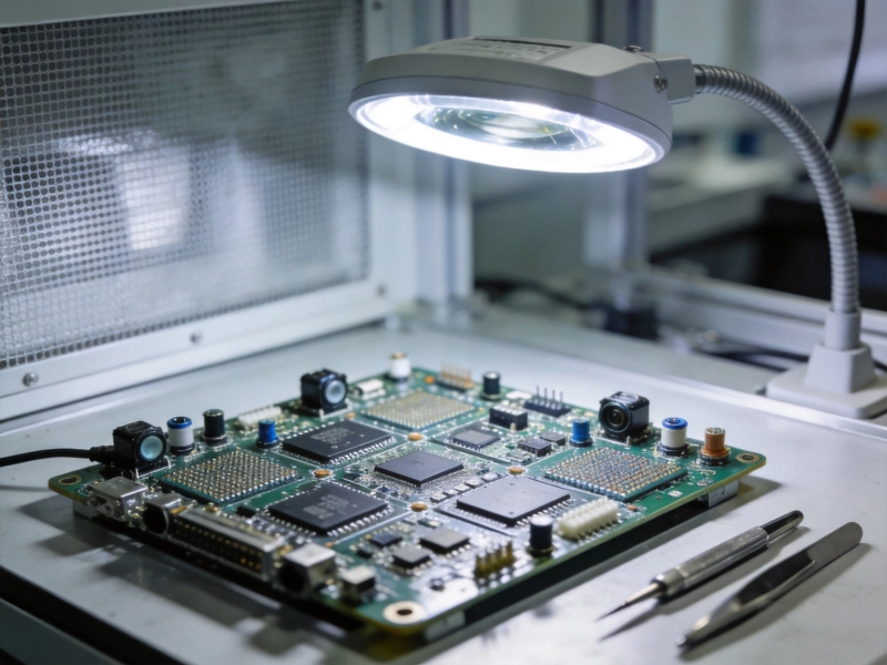
Turnkey PCB Assembly for Flight Control Systems and Navigation<June/22/2026
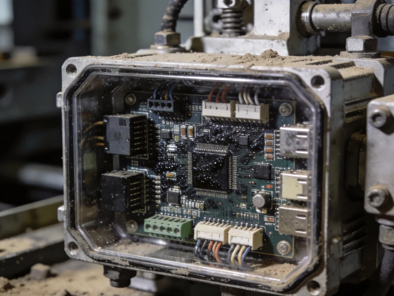
Ruggedized PCB Assembly for Harsh Industrial EnvironmentsJuly/20/2026

Expert Insights on Reducing Supply Chain Risks in Turnkey PCB AssemblyJune/03/2026

Best Turnkey PCB Assembly for Consumer & IoT ElectronicsJune/16/2026

Comprehensive Turnkey PCB Solutions for Complex Electronic SystemsJuly/14/2026

How Turnkey PCB Prototyping Reduces Development Cycles by 40%June/05/2026