Open Nav

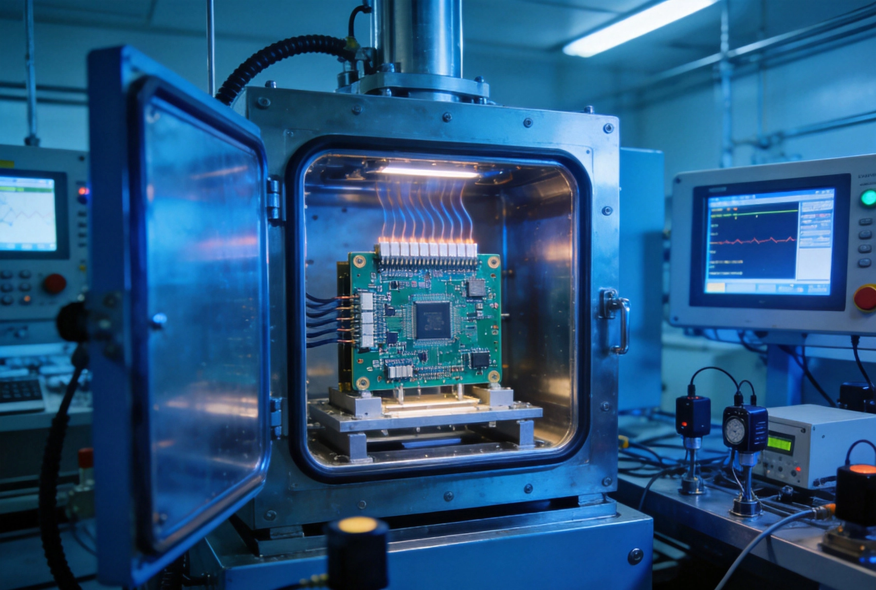
Aerospace printed circuit boards operate in conditions that would destroy ordinary electronics within minutes. Satellites orbiting Earth experience temperature swings exceeding 200 degrees Celsius between solar exposure and deep space shadow. Avionics systems in fighter jets endure sustained high-g vibration during maneuvering. Spacecraft face radiation levels that corrupt memory and degrade semiconductor performance. Each environment demands rigorous testing protocols that validate PCB assemblies will survive mission-critical operations without failure. Understanding these testing requirements helps engineers design for reliability and navigate the complex certification processes that govern Aerospace Electronics.
Aerospace applications place PCB assemblies under stresses rarely encountered in ground-based electronics. These environments combine multiple stressors simultaneously, creating synergistic effects more damaging than individual factors alone. A board might face radiation damage while cycling through extreme temperatures, with vibration stress further compromising structural integrity. This combination of simultaneous stressors distinguishes aerospace testing from industrial or Consumer Electronics qualification.
Mission duration adds another dimension of challenge. Consumer Electronics typically target three to five years of service life. Aerospace systems often require decades of reliable operation without maintenance access. A satellite launched today may need to function until 2050 or beyond, meaning every component and every solder joint must be qualified for extended life in environments that continuously degrade materials and junctions.
Commercial aircraft cruise at altitudes where atmospheric pressure is a fraction of sea level conditions. This reduced pressure lowers the breakdown voltage of air gaps, increasing susceptibility to corona discharge and arcing. PCBs designed for aerospace must account for these conditions through adequate spacing, Conformal Coating, and potting that eliminates air voids around sensitive components.
Partial discharge becomes a significant concern at altitude. When air pressure drops below approximately 75 kPa, microscopic voids in potting compounds or between PCB layers can experience localized ionization that gradually degrades insulation. Aerospace PCBs undergo partial discharge testing to identify and eliminate designs susceptible to this phenomenon that could cause mid-life failures.
Aerospace systems transition between vastly different humidity environments. An aircraft moving from tropical hangar conditions to high-altitude flight encounters dramatic humidity changes that can drive moisture into PCB materials. Military specifications address this through humidity bias testing that applies electrical stress during humidity exposure, accelerating failure mechanisms that might otherwise take years to manifest.
Pulse humidity testing using elevated temperature and pressure drives moisture into packages and interfaces more aggressively than natural aging. This testing identifies vulnerabilities in component packaging, underfill materials, and board coatings that could compromise long-term reliability. Boards passing pulse humidity tests demonstrate resilience against moisture-related failures in real-world service.
Temperature extremes define the most fundamental environmental challenge for Aerospace Electronics. Satellite electronics experience thermal cycles every 90 minutes as they pass between direct sunlight and the cold darkness of Earth's shadow. Aircraft electronics face similar cycles during flight profiles, with additional heating from internal power dissipation and engine proximity. Qualification testing must simulate these cycles accurately while accelerating time to failure.
Thermal testing encompasses multiple protocols addressing different failure mechanisms. Steady-state high temperature testing evaluates material stability and accelerated aging. Thermal cycling tests mechanical fatigue from repeated expansion and contraction. Thermal Shock Testing examines resistance to rapid temperature transitions that create internal stress gradients.
Aerospace thermal cycling tests typically specify -55°C to +125°C or wider ranges depending on application. Military standard MIL-PRF-55110 and space standard ECSS-Q-ST-70 provide detailed cycling requirements including ramp rates, dwell times, and cycle count targets. Commercial aerospace follows DO-160 environmental testing categories that define application-specific thermal requirements.
Cycle count requirements reflect the cumulative fatigue damage expected during service life. A satellite targeting 15-year operation might require qualification testing to 5,000 thermal cycles or more, representing accelerated simulation of orbital thermal stress. Boards must demonstrate no degradation in electrical performance, visual inspection, or X-ray examination after completing cycling sequences.
Space electronics face unique thermal vacuum conditions impossible to replicate at atmospheric pressure. In vacuum, heat transfer by convection disappears, leaving only radiation and conduction pathways. Components that cool adequately in air may overheat in vacuum, creating thermal design challenges that require careful analysis and testing validation.
Thermal vacuum testing places assemblies in vacuum chambers with precise temperature control using liquid nitrogen or liquid helium cooling. These tests validate thermal models, verify component derating assumptions, and identify hot spots created by the absence of convective cooling. Boards passing thermal vacuum testing have demonstrated survival in actual space conditions.
Aerospace platforms generate intense mechanical vibration during operation. Jet engine vibration frequencies couple through airframes into avionics compartments. Rocket launches impose extreme vibration and acoustic loads during the brief but violent launch phase. Launch vehicle separation events create shock impulses that stress circuit boards and their interconnections. Vibration testing validates that PCBs survive these mechanical environments.
Vibration test specifications define frequency ranges, acceleration levels, and test duration for different platform types. Random vibration testing applies simultaneous energy across a frequency spectrum, simulating complex real-world vibration environments. Sine sweep testing identifies resonant frequencies where boards or components amplify vibration inputs.
Shock Testing addresses brief high-energy events that impose sudden acceleration loads. Pyrotechnic separation events, crash landings, and emergency deployments create shock environments that can fracture solder joints, crack components, and delaminate PCB layers. Aerospace boards must pass shock tests demonstrating survival of representative impulse loads.
Shock response spectrum testing characterizes how boards respond to shock inputs across different frequencies. This analysis identifies vulnerable resonances and guides design modifications that reduce shock susceptibility. Pyroshock testing using explosive charges recreates the high-frequency shock content of actual separation events, providing the most realistic qualification testing available.
Real-world aerospace environments combine vibration with thermal cycling, humidity exposure, and electrical stress simultaneously. Combined environment testing applies multiple stressors concurrently, revealing failure mechanisms that single-factor testing might miss. Synergistic effects between thermal fatigue and vibration fatigue accelerate damage accumulation beyond simple superposition.
Highly Accelerated Life Testing (HALT) uses combined environments with escalating stress levels to rapidly identify design weaknesses. This testing does not replicate specific qualification requirements but instead explores design margins until failure occurs. Results guide design improvements that expand operational margins before formal qualification testing.
Space radiation poses unique challenges to electronic systems operating beyond Earth's protective atmosphere. Energetic particles from solar flares and cosmic rays cause single-event effects that corrupt data, latch up transistors, and gradually degrade materials. Aerospace PCBs must be designed and tested to withstand these radiation environments that have no ground-based equivalent.
Total ionizing dose testing evaluates cumulative radiation damage from prolonged exposure. Components and materials receive controlled radiation exposure in gamma ray or proton facilities, with electrical parameters monitored throughout. Dose levels target the total radiation expected during mission duration, typically ranging from kilorads to megarads depending on orbit and duration.
Single-event effects (SEE) result from individual radiation particles striking sensitive circuit nodes. Single-event latchup (SEL) creates spurious high-current states that can destroy devices if not quickly detected and reset. Single-event upset (SEU) corrupts memory bits, potentially changing program execution or corrupting data. Single-event transient (SET) creates voltage spikes that propagate through circuits as errors.
Heavy ion testing in particle accelerator facilities evaluates device susceptibility to single-event effects. Beams of heavy ions with well-defined energy and linear energy transfer (LET) properties simulate space radiation environments. Devices that latch up under testing require radiation-hardened alternatives or extensive mitigation circuitry to ensure reliable space operation.
High-energy particles cause displacement damage when they knock atoms from crystal lattice positions in semiconductor materials. This damage gradually reduces carrier mobility and increases leakage currents, progressively degrading device performance. Solar cell efficiency, optical sensor sensitivity, and bipolar transistor gain are particularly susceptible to displacement damage.
Proton and neutron testing evaluates displacement damage susceptibility in components that will operate in particle-rich radiation environments. Displacement damage dose (DDD) quantifies damage in terms of non-ionizing energy loss that creates lattice defects. Components must be characterized for DDD effects to enable accurate predictions of long-term performance degradation.
Beyond finished assembly testing, aerospace PCB qualification encompasses the materials and processes that create the board. Each material in the construction must be qualified for aerospace use, with documented traceability from raw material through finished assembly. This comprehensive qualification approach ensures that variations in material lots or process parameters cannot introduce reliability risks.
Base material qualification addresses the fundamental PCB substrate, including the resin system, reinforcement material, and any special features like high-temperature capability or radiation tolerance. Materials must demonstrate stability across temperature ranges, resistance to outgassing in vacuum, and long-term aging characteristics consistent with mission life requirements.
Materials in spacecraft undergo outgassing testing to ensure they do not release volatile compounds that could contaminate optical surfaces, sensors, or other sensitive equipment. Standard ASTM E595 testing measures collected volatile condensable materials (CVCM) and weight loss (WVR) when samples are heated in vacuum. Aerospace-grade materials must meet stringent limits on outgassing products.
Contamination Control extends beyond material selection to include manufacturing processes that might introduce contaminants. Flux residues, handling contaminants, and cleaning chemical residues all require evaluation for potential outgassing or corrosion issues. Many aerospace PCB manufacturers maintain dedicated cleanroom facilities that minimize contamination introduction during assembly.
The transition to lead-free solder alloys introduced new qualification challenges for aerospace applications. Tin whiskers, higher reflow temperatures, and different reliability characteristics compared to traditional tin-lead solders required extensive requalification of processes and materials. Many aerospace programs continue requiring lead-containing solders for their superior long-term reliability characteristics.
When lead-free processes are required, whisker mitigation strategies become essential. Pure tin plating and high-temperature reflow profiles promote whisker growth that can cause short circuits. Whisker mitigation involves tin alloy compositions, underlayer metals, and processing controls that reduce whisker propensity. Extensive testing verifies that mitigation approaches provide acceptable reliability for the intended application.
Aerospace PCBs require comprehensive documentation demonstrating that every aspect of design, materials, and manufacturing meets applicable requirements. This documentation package supports certification processes, enables traceability, and provides evidence of compliance for regulatory authorities and customers. Maintaining complete records throughout product life is essential, as some aerospace systems remain in service for decades.
First Article Inspection (FAI) documentation captures initial production conformance to design specifications. This comprehensive record includes dimensional measurements, electrical test results, visual inspection findings, and any special process verifications. FAI packages provide reference standards against which subsequent production is compared, enabling change detection and configuration control.
Aerospace electronics follow stringent workmanship standards that define acceptable quality levels for solder joints, component attachment, Conformal Coating, and marking. Ipc Standards provide baseline workmanship criteria, while aerospace-specific standards like NASA-STD-8739 and J-STD-001 establish elevated requirements for mission-critical assemblies.
Acceptance criteria specify defect limits and inspection requirements for each assembly characteristic. These criteria must be measurable and unambiguous to enable consistent decisions across different inspectors. Digital inspection systems increasingly supplement human visual examination, providing objective measurement and improved repeatability for critical parameters.
Configuration management ensures that documentation accurately reflects as-built hardware throughout production and sustainment. Change control processes evaluate proposed modifications for impact on form, fit, function, and interface compatibility. Proposed changes that affect these characteristics require formal review and approval before implementation.
Complete traceability links finished assemblies to their constituent components, materials, manufacturing processes, and inspection records. This traceability enables investigation when field failures occur, supporting root cause analysis and corrective action. Aerospace traceability requirements often extend back through multiple supplier levels to raw material certifications.
Aerospace Pcb Testing imposes substantial costs and extends development schedules significantly beyond commercial electronics timelines. Environmental testing facilities, radiation test facilities, and qualification laboratories charge premium rates for their specialized capabilities. Extended test programs lasting months or years require sustained funding and program commitment.
Design modifications discovered during qualification testing can trigger costly and time-consuming iterations. Finding and fixing problems early through design reviews and analysis reduces this risk, but some issues remain undetectable until physical testing exposes them. Managing qualification program risk through phased testing approaches and design margins helps control costs while maintaining schedule confidence.
Traditional qualification testing builds and tests separate qualification units that are destroyed during testing, with production units following a separate build process. Protoflight testing qualifies production-representative hardware through a combined qualification and acceptance test program. This approach reduces total unit counts and program cost while accepting some risk that production processes might not exactly match qualification hardware.
Choosing between qualification approaches depends on program risk tolerance, budget constraints, and criticality of the hardware. Human-rated systems typically require traditional qualification with margin testing that pushes hardware beyond specification limits. Unmanned systems with limited budgets may accept protoflight approaches that reduce development cost at some acceptance risk.
Extreme environment testing for aerospace Pcb Assembly represents the most demanding qualification process in the electronics industry. Thermal cycling, vibration, radiation, and combined environment testing validate that circuit boards will perform reliably in conditions far beyond commercial electronics experience. This comprehensive testing protects human life, preserves expensive platforms, and enables mission success in the most challenging operating environments imaginable.
Engineers designing for aerospace applications must understand these testing requirements from the earliest design phases. Materials selection, component derating, thermal design, and structural considerations all influence whether designs will pass qualification testing. Early collaboration with testing laboratories and qualification experts helps identify potential issues before they become expensive problems discovered late in programs.
The investment in aerospace PCB qualification reflects the extraordinary stakes of space and aviation systems. When satellites, aircraft, and spacecraft operate reliably for years or decades, the thorough qualification testing that enabled that reliability pays dividends many times over. For engineers and program managers navigating aerospace electronics development, understanding these testing requirements is essential knowledge for creating systems that perform when failure is not an option.
Best Turnkey PCB Assembly for Aerospace, Defense & Avionics: MIL-STD ComplianceJuly/22/2026
The Trade-offs Between Speed and Cost in Rapid Turnkey PCBAJuly/13/2026
Turnkey PCB Assembly for Flight Control Systems and Navigation<June/22/2026
5 Common Mistakes to Avoid During Turnkey PCB PrototypingJuly/07/2026

Best Turnkey PCB Assembly Services: Balancing Cost, Quality, and SpeedJuly/01/2026
What Are Turnkey PCB Services?May/26/2026
The Role of Low Volume Turnkey PCBA in Market ValidationSeptember/08/2026
Quality Control Standards in Turnkey SMT Assembly (IPC-A-610 Explained)July/07/2026