
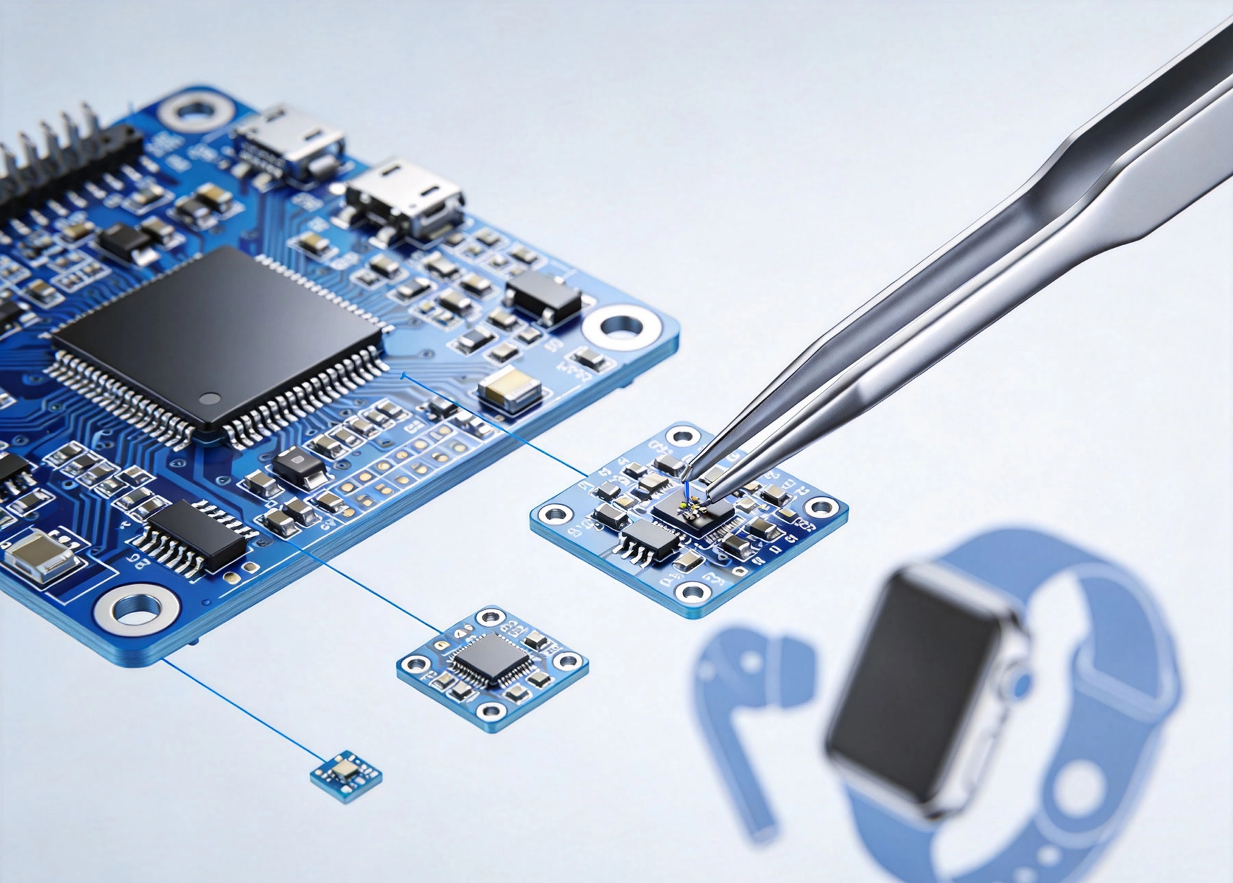
Your smartwatch monitors your heart rate while your earbuds deliver crystal-clear audio—all from devices smaller than a matchbox. This remarkable feat of engineering didn't happen by accident. Behind each wearable lies intense engineering battles fought in fractions of millimeters.
Turnkey PCB Assembly for wearables faces challenges that differ fundamentally from traditional Electronics Manufacturing. Space constraints collide with thermal limits, battery capacity wars with safety requirements, and component availability struggles against the relentless demand for smaller, lighter, more capable devices.
If you're designing wearable electronics or sourcing assembly services for these products, understanding these challenges helps you make better design decisions and choose partners who can actually deliver.
Consumer expectations drive wearables toward invisible form factors. Smart rings that track sleep. Hearing aids disguised as fashion accessories. Patches that monitor glucose continuously. Each product category pushes the boundaries of what engineers can squeeze into comfortable, wearable shapes.
PCB designers for wearables operate in spatial regimes that traditional electronics engineers rarely encounter. While consumer gadgets might optimize for cost within reasonable size targets, wearables optimize for size first—cost is secondary to fitting inside a watch band, ear canal, or ring shank.
A smartwatch motherboard might occupy 4cm². A fitness tracker perhaps 2cm². An earbud processing board? Sometimes under 0.5cm². These aren't incremental improvements—they represent order-of-magnitude reductions from typical PCB designs.
Every square millimeter demands justification. Passive components that disappear in larger designs become conspicuous space hogs here. The 0201 resistor you ignored on previous boards becomes a layout problem requiring careful planning.
Wearables are thin—typically 5mm to 10mm total thickness. This constraint interacts badly with battery requirements, display modules, and sensor placement. PCB thickness options (0.4mm to 1.6mm standard) suddenly become critical decisions that ripple through the entire mechanical design.
Flexible circuits offer relief but introduce new manufacturing challenges. Rigid-flex assemblies for wearables require careful stress analysis and manufacturing processes that differ significantly from standard rigid board production.
Choosing components for wearable PCBs requires a different mindset than typical electronics procurement.
Standard component packages—0603, 0805, SOIC—may simply not fit. Designers must specify the smallest available packages:
The component datasheet specifications you relied on for larger designs become less relevant. Thermal performance, for instance, assumes larger packages with better heat spreading—conditions that don't apply to tiny WLCSP devices.
Small packages often have longer lead times than standard versions. A microcontroller might be available in SOIC with 8-week lead time but the WLCSP version requires 20 weeks. Supply Chain planning for wearables requires months of visibility that many companies lack.
Second-source options shrink dramatically at smaller packages. Finding an alternative microcontroller with identical pinout in a smaller footprint is rarely possible. This creates Supply Chain vulnerability that product managers must acknowledge and manage.
Heat dissipation becomes problematic in small packages. Standard ICs rely on copper planes and larger pads to spread thermal energy. WLCSP packages have no lead frame—their only thermal path is directly through the substrate into the PCB.
Thermal simulation that seemed optional for larger designs becomes essential for wearables. The concentrated heat output of processors in tiny packages can cause reliability failures or safety issues if not properly managed.
Thermal Management for wearables differs fundamentally from larger electronics.
Traditional Thermal Management adds metal clips, thermal pads, and dedicated heat sinking structures. In a smartwatch? No room. Every cubic millimeter competes with the battery, display, and sensors that define the product's value.
Wearable thermal management must work through the board itself. Thermal vias, copper coin embedding, and substrate engineering become primary tools. Some manufacturers use metal-core substrates that provide thermal paths without discrete components.
Unlike most electronics, wearables operate in contact with human skin. This introduces a critical safety constraint: surface temperatures must stay below 45°C to prevent burns during prolonged contact. This limit is far below typical electronics operating temperatures.
Processor-intensive tasks—GPS tracking, cellular connectivity, health algorithm computation—can push component temperatures beyond safe limits. Thermal throttling, processor duty cycling, and software optimization become necessary to maintain safe skin temperatures.
Rather than centralizing processing in one powerful chip, wearable designs often distribute workloads across multiple smaller processors. This reduces heat concentration at any single point but increases board complexity and component count.
Some designs include dedicated microcontrollers for specific functions (sensors, wireless, display) that sleep when inactive. This approach reduces average power consumption and heat generation, trading increased BOM complexity for thermal and power benefits.
Battery capacity drives wearable utility—but capacity requires volume, and volume is scarce.
Wearable batteries rarely resemble standard cylindrical or prismatic cells. They must conform to product shapes: curved batteries for watches, thin flexible batteries for patches, cylindrical-miniature cells for hearing aids.
PCB designers must accommodate these unconventional battery shapes and placements. Battery management circuits must work with varying cell chemistries and form factors, often in configurations that complicate balancing and protection circuitry.
Lithium-polymer batteries in wearable form factors require careful safety considerations. Punctures, crushes, or charging faults can cause thermal runaway in these compact cells. Protection circuits must monitor voltage, current, and temperature with failsafe responses that prevent hazardous conditions.
Assembly processes must include specific precautions for battery handling: ESD protection, avoiding sharp tooling near cells, and controlled heating during any reflow operations that might affect battery integrity.
Eliminating charging connectors simplifies wearable enclosures but adds PCB complexity. Wireless charging receiver coils require precise placement relative to the charger, often with ferrite backing to direct magnetic flux and improve efficiency.
The receiver coil, associated circuitry, and protection components occupy board space that could otherwise serve primary functions. Balancing charging efficiency against space constraints is an ongoing optimization challenge.
Rigid-flex PCBs have become nearly mandatory for advanced wearables.
Rigid-flex assemblies stack functional areas in three dimensions rather than spreading them across a flat plane. A watch might use a rigid main board folded behind the display, with a flexible section connecting to a sensor board in the watch band.
This approach saves horizontal space but demands careful mechanical integration. The flexible sections experience repeated bending during product assembly and use, requiring strain relief and controlled bend radii.
Rigid-flex PCBs cost more and require specialized manufacturing capabilities. The interface between rigid and flexible sections—the "hinge zone"—represents the most common failure point. Careful design, appropriate material selection, and process control during assembly prevent field failures.
Not all Turnkey Assembly providers can handle rigid-flex work. Those that do often have minimum order quantities or tooling charges that only make sense for higher-volume products. Evaluating your assembly partner's actual rigid-flex capability matters enormously.
Flexible sections must endure repeated bending without conductor fatigue. Polyimide substrates (Kapton) provide excellent flexibility and temperature resistance. However, polyimide absorbs moisture, requiring special handling during assembly to prevent delamination or blistering during reflow.
Some designs use rigid-flex-rigid configurations that provide component mounting flexibility in the middle section while using rigid boards for areas requiring stable mounting surfaces. These hybrid constructions balance mechanical flexibility against assembly convenience.
Wearables need wireless connectivity—typically Bluetooth for phone communication and sometimes additional protocols for specialized functions.
Antennas require specific clearance volumes to function efficiently. In larger devices, this space is easy to provide. In a smartwatch or earbud, Antenna Design becomes a serious challenge that interacts with PCB layout, mechanical enclosure, and human body proximity.
Body proximity affects antenna performance significantly. The human body absorbs RF energy, detuning antennas and reducing range. Designers must simulate or measure antenna performance with realistic body presence, accounting for different wearing positions and clothing layers.
RF circuits require careful Signal Integrity management. Transmission lines, ground planes, and component placement all affect Wireless Performance. At Bluetooth frequencies, these considerations are manageable, but still demand attention that traditional digital designers may overlook.
Balancing RF requirements against space constraints creates tradeoffs everywhere. Larger ground planes improve antenna efficiency but consume board space. Component placement for optimal RF may conflict with thermal or mechanical requirements.
Wireless devices require regulatory certification: FCC in the United States, CE in Europe, and equivalents elsewhere. These certifications test emissions, immunity, and specific absorption rate (SAR) for devices worn on the body.
SAR limits constrain maximum transmit power, directly affecting wireless range. Meeting SAR limits in a small form factor while maintaining adequate range requires careful Antenna Design and sometimes lower-power chipset selection.
Wearables face reliability challenges that exceed typical Consumer Electronics.
Unlike most electronics that sit stationary, wearables experience ongoing mechanical stress: putting on and removing watches, the constant motion of fitness trackers, insertion and removal of earbuds. PCBs and solder joints must survive these repeated stress cycles.
Shock and vibration testing for wearables may use different profiles than industrial or automotive applications. Talk with your assembly partner about realistic use-case testing that matches how consumers actually treat these devices.
Wearables encounter moisture: sweat during exercise, rain during commutes, accidental submersion for some devices. Conformal Coating, waterproof connectors, and hydrophobic PCB coatings help protect assemblies, but add cost and assembly complexity.
IP67 or IP68 ratings require comprehensive sealing strategies that affect PCB layout, connector selection, and assembly sequencing. Sacrificial waterproofing during assembly (using temporary seals removed after processing) adds manufacturing steps and cost.
Consumers expect wearables to function reliably for years. The battery may need replacement, but the electronics should outlast device更换 cycles. This reliability expectation demands higher-quality assembly practices than disposable electronics—comparable to automotive or medical standards.
Successful wearable products require design and manufacturing to work together from the start.
Waiting to involve your assembly partner until design is complete often causes problems. Component selection, thermal management strategy, and flex circuit design all benefit from manufacturing input during the concept phase.
Turnkey Assembly providers experienced with wearables can identify potential issues before they become expensive revisions. Their knowledge of component availability, assembly capabilities, and test coverage prevents problems that would surface only during production.
Small board size limits access for test probes. Boundary scan testing becomes more valuable when physical probe access is limited. Flying probe testing with smaller probe pitches handles most testing needs, but requires fixturing that may not exist for novel board shapes.
Functional test coverage requires creative approaches when in-circuit test is impractical. Some wearable assemblies rely heavily on functional test at the module or finished-goods level rather than individual board testing.
Rigid-flex assemblies and high-density designs severely limit rework capability. A failed component on a rigid-flex board may require returning the entire assembly to a specialized rework facility. Plan for this reality by designing for maximum first-pass yield rather than assuming rework will fix problems.
Not all turnkey providers handle wearables equally well. Evaluate potential partners carefully.
Ask specifically about their experience with:
General Ems experience doesn't automatically translate to wearable expertise. Look for documented success with similar products.
ISO 9001 provides baseline quality system assurance. For medical or regulated wearable products, Iso 13485 or specific device certifications may be required. Ask about their quality metrics for small-format assemblies—are defect rates tracking separately from larger boards?
Component access matters for wearables. Partners with direct distributor relationships get allocation priority during shortages. Their ability to source small-package components—often from different suppliers than your larger-product programs—indicates genuine wearable supply chain capability.
Miniaturization in wearable electronics represents one of the most demanding challenges in modern Electronics Manufacturing. Success requires simultaneous optimization across thermal management, battery integration, Wireless Performance, and mechanical reliability—all while maintaining acceptable costs and production yields.
The path forward demands tight integration between design, supply chain, and manufacturing. Component selection affects thermal performance. Thermal design influences component selection. Assembly capabilities constrain mechanical design. Everything connects.
Choosing a turnkey assembly partner early in development—ideally during concept phase—transforms these challenges from obstacles into manageable engineering problems. Partners with demonstrated wearable expertise bring component knowledge, process capability, and test coverage that improves first-pass yield and Time-to-market.
The wearables market continues evolving rapidly. New sensor types, wireless protocols, and form factors create ongoing engineering challenges. But for companies willing to invest in the specialized expertise these products demand, the market rewards continue to grow.
Wearable PCBs typically range from 0.4mm to 0.8mm total thickness. Thinner boards save space but become more fragile and harder to handle during assembly. Your assembly partner's capabilities and the product's mechanical requirements should drive this decision.
Thermal management combines multiple approaches: thermal vias and copper weights to spread heat through the board, processor duty cycling to limit sustained power dissipation, software thermal throttling when temperatures rise, and careful placement that keeps heat sources away from skin-contact surfaces.
Small-format wearable boards typically see 2% to 5% lower first-pass yield than standard Consumer Electronics. The difference reflects handling challenges, component placement precision requirements, and limited rework options. This yield gap makes manufacturing learning curve investments and first-pass design verification particularly important.
Yes, but testing approaches differ from rigid boards. Boundary scan testing provides good coverage for circuits with limited physical access. Flying probe testing handles many test requirements with appropriate fixturing. Functional test at the module or finished-goods level fills remaining coverage gaps.
Conformal Coating provides valuable moisture and corrosion protection for many wearables, but isn't always required. Products with high IP ratings (IP67+) typically need coating plus comprehensive sealing. Products rated only for splash resistance may rely on enclosure sealing alone. Your use-case requirements and target market should drive this decision.
Most common failure modes involve underestimated manufacturing complexity: thermal issues discovered too late, rework capability gaps revealed during yield problems, or supply chain surprises with small-package components. Early involvement of experienced assembly partners prevents most of these issues.
This article is intended for informational purposes. Consult with qualified electronics design engineers and experienced wearable assembly partners for specific application requirements.
Ensuring Wireless Performance in IoT Turnkey PCB AssemblySeptember/14/2026

Zero-Defect Strategies in Turnkey PCB Assembly for Safety-Critical Auto PartsOctober/19/2026
Low Volume Turnkey PCBA: Flexibility for Niche and Specialized MarketsJuly/09/2026

Comprehensive Turnkey PCB Solutions for Complex Electronic SystemsJuly/14/2026

Cleanroom Manufacturing Standards for Implantable Medical PCBAJuly/21/2026

Cost-Effective Turnkey PCB Assembly Strategies for Smart Home DevicesAugust/06/2026

The Ultimate Guide to Turnkey PCB Prototyping for Hardware EngineersMay/26/2026

Essential Questions to Ask Before Hiring Turnkey PCB ServicesSeptember/26/2026