
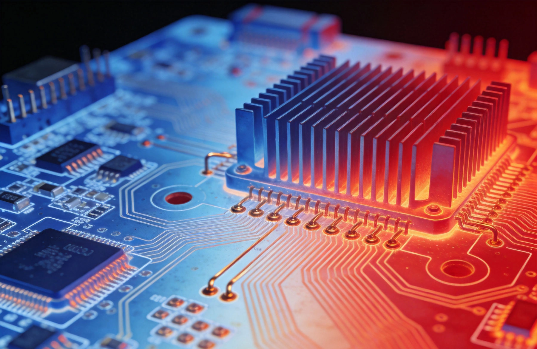
Power Electronics operate at the edge of physical limits. Components dissipate substantial energy as heat while maintaining precise electrical performance. Whether designing motor drives, solar inverters, battery management systems, or LED lighting, Thermal Management determines whether your product functions reliably or fails prematurely. The printed circuit board itself becomes an active Thermal Management element, and mastering heat flow through PCB architecture distinguishes successful Power Electronics designs from those plagued by field returns and reliability problems.
Effective thermal management begins with understanding where heat originates. Power electronics convert energy forms and regulate voltages and currents, and every conversion process generates waste heat proportional to inefficiency. A 90% efficient power converter operating at 100W output dissipates 10W as heat—seemingly modest until that heat concentrates in a few square centimeters of board space.
Semiconductors generate the majority of heat in most power circuits. MOSFETs and diodes contribution significant losses during switching transitions and conduction phases. High-side gate drivers, current sense amplifiers, and voltage regulators each contribute according to their power consumption and thermal design margins.
Copper traces and planes carrying high currents generate heat through resistive losses. While typically minor compared to semiconductor dissipation, poorly designed high-current paths in power distribution networks create localized hot spots that compound thermal problems.
Semiconductor parameters shift with temperature in predictable but problematic ways. MOSFET on-resistance increases approximately 0.5% per degree Celsius—modest per degree but substantial over 100°C operating ranges. Junction temperatures approaching limits cause thermal runaway in some configurations, where increased temperature causes increased losses, causing further temperature rise.
Electrolytic capacitors age exponentially faster at elevated temperatures. A capacitor specified for 5000 hours at 105°C might last 50,000 hours at 65°C operating temperature. Thermal management directly impacts product lifetime.
Copper's thermal conductivity exceeds that of many metals—approximately 400 W/m·K compared to aluminum at 237 W/m·K or steel at 17 W/m·K. Strategic copper deployment on PCBs provides substantial heat spreading capability without adding discrete components.
Copper planes beneath or adjacent to heat-generating components provide thermal paths spreading heat across larger areas. The spreading resistance from a concentrated heat source to a larger plane area dramatically reduces thermal resistance to ambient conditions.
Designers must account for effective thermal conductivity through PCB stackups. Standard FR-4 laminate conducts heat poorly—approximately 0.3 W/m·K—meaning thermal paths through dielectric layers create substantial resistance. Thermal vias or direct copper contact provide lower-resistance paths through the board to planes on opposite sides.
Heavier copper handles current more efficiently while also spreading heat better. A 2 oz/sq ft copper plane spreads heat approximately 40% more effectively than 1 oz copper due to increased cross-sectional area for heat flow. However, fabrication costs increase with copper weight, and excessive copper creates challenges for fine-pitch component assembly.
Strategic copper weighting—using heavy copper for thermal planes while maintaining standard weights for signal layers—balances thermal performance against manufacturing cost. Many manufacturers offer mixed copper weights within the same stackup, enabling optimized thermal designs without universal heavy copper pricing.
Thermal vias connect copper features across PCB layers, providing critical thermal paths that dramatically reduce junction-to-ambient resistance.
Placing thermal vias directly beneath component pads connects the component thermal interface to internal and bottom-layer copper planes. Via arrays surrounding high-power packages provide parallel thermal paths that collectively handle substantial heat flows.
Via diameter and plating thickness determine thermal resistance. Larger vias with heavy plating provide lower resistance but consume board area and may interfere with routing. Typical thermal via arrays use 0.3-0.5mm diameter vias on 0.8-1.2mm spacing—sufficient thermal performance without compromising board real estate.
Unfilled vias create reliability risks from solder wicking during assembly. Molten solder draws into via barrels through capillary action, potentially creating insufficient solder joints or voids compromising electrical and thermal performance.
Via filling using conductive or non-conductive epoxies addresses solder wicking while maintaining thermal conductivity. Conductive filled vias provide continuous thermal paths but cost more. Non-conductive fill with copper over-plating offers compromise performance at moderate pricing. Some designs simply use solder mask covering vias, which provides minimal thermal benefit but prevents solder wicking.
When PCB copper cannot sufficiently spread heat, discrete heatsinks provide additional thermal capacity. Multiple attachment methods achieve different trade-offs in thermal performance, cost, and manufacturing complexity.
h3>Through-Hole Lead SolderingLead-form components accepting heatsinks often feature through-hole leads that provide robust thermal and mechanical connections. Soldering leads into vias with thermal pads creates reliable thermal paths but limits flexibility and complicates rework.
This approach suits high-volume production where assembly costs remain acceptable and field reliability justifies manufacturing complexity. Automotive and industrial applications frequently employ through-hole thermal connections for their proven reliability under thermal cycling and vibration stress.
Bottom-thermal-pad packages like QFN, DFN, and thermally-enhanced SOIC mount directly to PCB copper pads providing thermal interfaces. These packages achieve impressive thermal performance without through-hole complexity.
Thermal pad solder coverage determines thermal resistance. Incomplete solder wetting creates voids increasing thermal resistance and potentially causing mechanical delamination under thermal cycling. Void area generally should remain below 10% for optimal thermal and reliability performance.
Clip-attached heatsinks provide serviceable thermal enhancement without permanent attachment. Spring clips apply consistent pressure maintaining thermal interface material performance throughout product lifetime. This approach suits products requiring field serviceability or applications where thermal requirements might change during product lifecycle.
Thermal interface materials between heatsink and component or PCB surface compensate for surface flatness variations. Materials range from basic thermal pads to phase-change compounds that liquefy at operating temperatures, filling microscopic surface irregularities for improved thermal contact.
The interface between components and heatsinks or thermal planes introduces thermal resistance that proper material selection can minimize.
Pre-cured thermal pads provide consistent thickness and straightforward assembly. These materials compress slightly under mounting pressure, accommodating surface irregularities while maintaining electrical isolation where required. Typical thermal conductivity ranges from 1 to 8 W/m·K depending on material formulation.
Gap fillers provide similar function for variable spacing between components and heatsinks. These pumpable materials fill cavities and conform to irregular surfaces, useful when component heights vary or when multiple components require thermal connection to a common heatsink.
Thermal grease provides lowest thermal resistance of common interface materials but requires careful application to avoid pump-out from thermal cycling. Silicone-based greases resist drying but may migrate under vibration. Non-silicone alternatives avoid potential compatibility issues but require more careful application.
Phase-change materials offer attractive middle-ground performance. Solid at room temperature, these materials liquefy at operating temperatures, achieving thermal contact approaching grease performance while maintaining handling convenience of solid pads. They resist pump-out better than grease due to their solid-room-temperature state.
Passive thermal management suffices for many applications, but demanding power levels require active cooling approaches.
Fans provide additional convective heat transfer when passive cooling reaches limits. Even modest air flow dramatically improves heatsink effectiveness by preventing hot air accumulation and maintaining temperature differential driving heat transfer.
Thermal simulation helps optimize fan placement and airflow routing. Channeling air across heatsink fins efficiently removes heat while improperly routed airflow provides minimal benefit. Computational fluid dynamics tools model airflow and thermal performance, guiding design decisions for complex enclosures.
Water-cooled cold plates attached to PCBs provide highest thermal performance for extreme power applications. Liquid cooling enables heat removal rates impossible with air cooling, but adds system complexity, potential leakage risks, and ongoing maintenance requirements.
Miniature water-cooled structures integrated into PCB assemblies serve niche applications where size constraints preclude air-cooled solutions. These approaches remain rare due to complexity but represent viable options for specialized high-power systems like electric vehicle chargers or industrial laser drivers.
Modern design workflows incorporate thermal simulation early, identifying problems before physical prototypes reveal expensive surprises.
Thermal simulation software models heat generation, conduction through PCB materials, convection from surfaces, and radiation where relevant. Tools from Ansys, Siemens, Cadence, and specialized PCB thermal packages provide varying capability levels suitable for different design stages.
Early design stages benefit from simplified thermal analysis focusing on critical paths and approximate material properties. Detailed simulation during final design verification accounts for complex geometries, material anisotropies, and boundary conditions more accurately.
Thermal imaging cameras verify simulation predictions and identify unexpected hot spots in prototypes. Infrared thermography reveals temperature distribution across PCB surfaces, guiding design iterations and identifying areas requiring additional thermal enhancement.
Thermocouples placed on actual components and boards provide point temperature measurements supplementing thermal imaging. Combining these techniques builds confidence that thermal designs meet requirements under worst-case operating conditions.
Thermal management techniques introduce manufacturing requirements that must align with assembly capabilities.
Thermal vias create challenges for Solder Paste application and Reflow Soldering. Paste may deposit into via barrels rather than on component pads, causing insufficient solder at joints. Common techniques include using Solder Paste stencils with small holes over thermal vias or accepting some solder loss into vias while ensuring adequate paste remains for reliable joints.
Heavy copper requires adjusted reflow profiles accounting for increased thermal mass. Soak times and peak temperatures may require modification to ensure uniform heating through Thick Copper regions. Coordinate with your Contract Manufacturer to establish appropriate profiles for thermal-enhanced designs.
Thermal via quality directly impacts assembly reliability. Automated Optical Inspection verifies solder paste coverage and joint formation. X-ray inspection examines hidden solder joints under bottom-thermal-pad packages, ensuring adequate thermal interface formation.
Thermal interface material application requires quality control processes ensuring proper coverage without voids. Automated dispensing systems provide consistent material placement while manual application requires skilled operators and inspection protocols.
Thermal management must account for product lifetime expectations, not merely initial performance.
Products operating across temperature ranges experience thermal cycling that stresses solder joints, thermal interfaces, and PCB materials. Each thermal cycle creates small damage accumulations potentially leading to eventual failure. Designs must account for expected thermal cycling severity over product lifetime.
Thermal vias and heavy copper create coefficient of thermal expansion mismatches potentially accelerating fatigue. Proper design distributes strain and avoids stress concentrations that cause crack propagation. Thermal cycling tests validate designs before production release.
Designing thermal systems with margin provides robustness against unexpected operating conditions. Components approaching thermal limits under nominal conditions leave no buffer for component variation, unusual loading, or elevated ambient temperatures. Designs operating at 70% of maximum rated junction temperature provide substantially greater reliability headroom.
Thermal management in Power Electronics Pcb assembly combines physics, materials science, and manufacturing engineering into practical design practices. Effective thermal designs incorporate heat spreading through copper, thermal vias connecting layers, strategic heatsink integration, and appropriate thermal interface materials—all integrated with manufacturing capabilities and reliability requirements.
Start thermal planning early in the design process. Define power budgets, identify critical components, and establish thermal budgets allocating permissible temperature rises across thermal paths. Early simulation guides architecture decisions that become expensive to change later.
Prototype validation confirms simulation accuracy and reveals issues not captured in models. Thermal imaging and direct temperature measurements verify designs meet requirements under worst-case conditions. Iterate designs until measurement confirms predictions.
Manufacturing alignment ensures thermal designs translate into reliable products. Work with assembly partners experienced in thermal-enhanced designs. Their expertise in handling thermal vias, heavy copper, and thermal interface materials prevents issues that undermine thermal performance.
Power electronics success depends on managing heat as a first-class design constraint. Invest in thermal management with the same rigor applied to electrical performance, and your products will deliver reliable performance throughout their intended lifetimes.
Custom Turnkey PCB Solutions for Harsh Environment ApplicationsSeptember/11/2026
Best Turnkey PCB Assembly for Energy & Power Electronics: Handling High VoltageJune/17/2026
Heavy Copper PCBs: Assembly Challenges and SolutionsAugust/07/2026
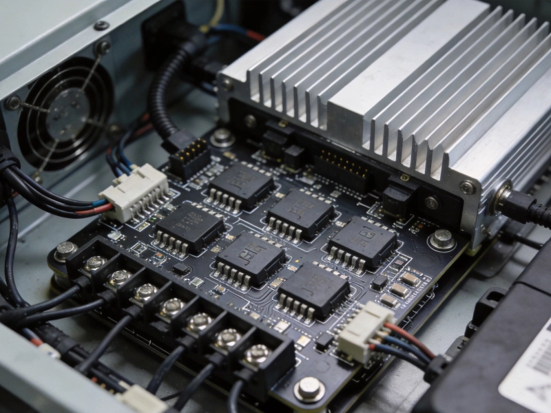
Best Turnkey PCB Assembly for EV Charging Stations and InvertersSeptember/15/2026
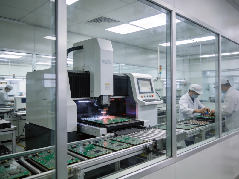
Why Transparency is the Key Feature of the Best Turnkey PCB Assembly ProvidersJuly/24/2026
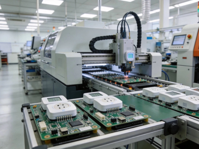
Cost-Effective Turnkey PCB Assembly Strategies for Smart Home DevicesAugust/06/2026
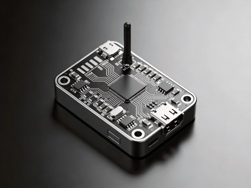
Ensuring Wireless Performance in IoT Turnkey PCB AssemblySeptember/14/2026

High Volume Turnkey PCBA: The Importance of Automated Assembly LinesSeptember/09/2026