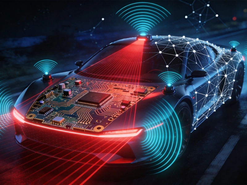
In the fast-paced world of electronics development, time is often the most critical resource. Engineers and product managers are constantly seeking ways to reduce lead times without compromising quality. This is where Turnkey Pcb Manufacturing has become the industry standard. Unlike traditional models where you might source bare boards from one vendor, components from another, and assembly from a third, turnkey services consolidate the entire Supply Chain into a single point of accountability.
But what exactly happens behind the scenes when you upload your Gerber files and BOM (Bill of Materials) to a turnkey provider? Understanding this workflow is essential for optimizing your designs for manufacturability (DFM) and ensuring a smooth production run. Here is a detailed walkthrough of the modern turnkey Pcb Manufacturing lifecycle.
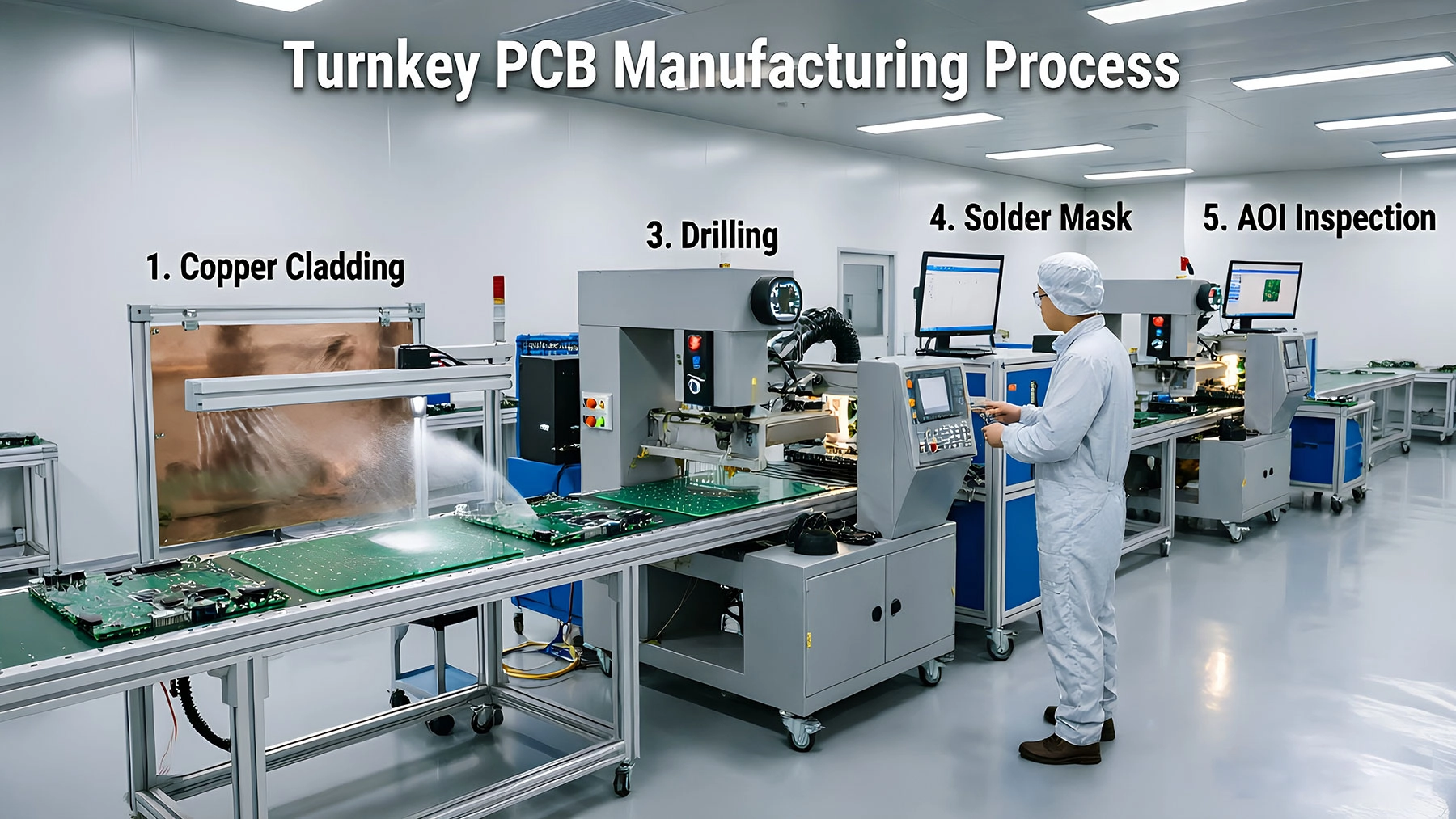
The process begins long before any copper is etched. Once the order is placed, the manufacturer’s engineering team performs a rigorous Design for Manufacturability (DFM) check. This automated and manual review scans your Gerber files for potential pitfalls—such as traces that are too close together, vias that might cause soldering issues, or silkscreen overlapping pads.
Simultaneously, the procurement team analyzes your BOM. In a true turnkey model, they verify component availability, check for obsolete parts, and suggest alternatives if necessary. This proactive step prevents the dreaded "line down" scenario where assembly halts because a single capacitor is out of stock.
With the design validated, fabrication begins. This involves several precise chemical and mechanical steps:
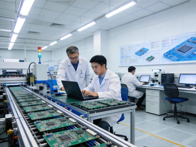
While the boards are being fabricated, the Supply Chain team is busy sourcing components. In a turnkey setup, the manufacturer leverages their relationships with global distributors (like Digi-Key, Mouser, or direct factory channels) to purchase parts at scale. All components are received, inspected for authenticity, and "kitted"—organized into trays or reels specifically for your project's assembly run.
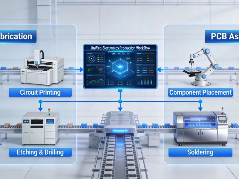
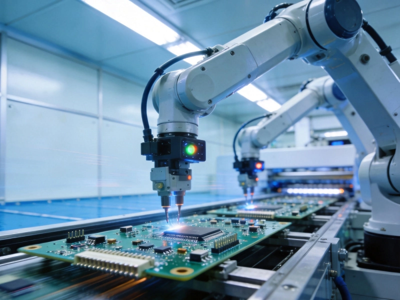
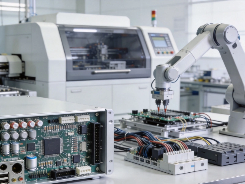
This is where the bare board transforms into a functional electronic unit. The assembly process typically follows this sequence:
A turnkey provider doesn't just ship boxes; they ship verified functionality. Depending on the service level selected, this phase includes:
The Turnkey Pcb manufacturing process is a symphony of logistics, chemistry, and robotics. By integrating fabrication, sourcing, and assembly under one roof, it eliminates the friction of managing multiple vendors. For hardware startups and established enterprises alike, mastering this workflow is the key to getting innovative products to market faster and more reliably.
Turnkey PCB Manufacturing: Integrating Fabrication and Assembly SeamlesslyMay/26/2026
Turnkey PCB Manufacturing for Rigid-Flex and HDI BoardsJuly/08/2026
Rapid Turnkey PCBA: How to Get Your Electronics Built in Days, Not WeeksJune/15/2026
Comprehensive Turnkey PCB Solutions for Complex Electronic SystemsJuly/14/2026
How to Choose the Best Turnkey PCB Assembly Partner in 2026May/26/2026
Best Turnkey PCB Assembly Services: Balancing Cost, Quality, and SpeedJuly/01/2026
Miniaturization Challenges in Turnkey PCB Assembly for WearablesJuly/15/2026
The Role of Turnkey PCB Assembly in Advanced Driver Assistance Systems (ADAS)July/17/2026